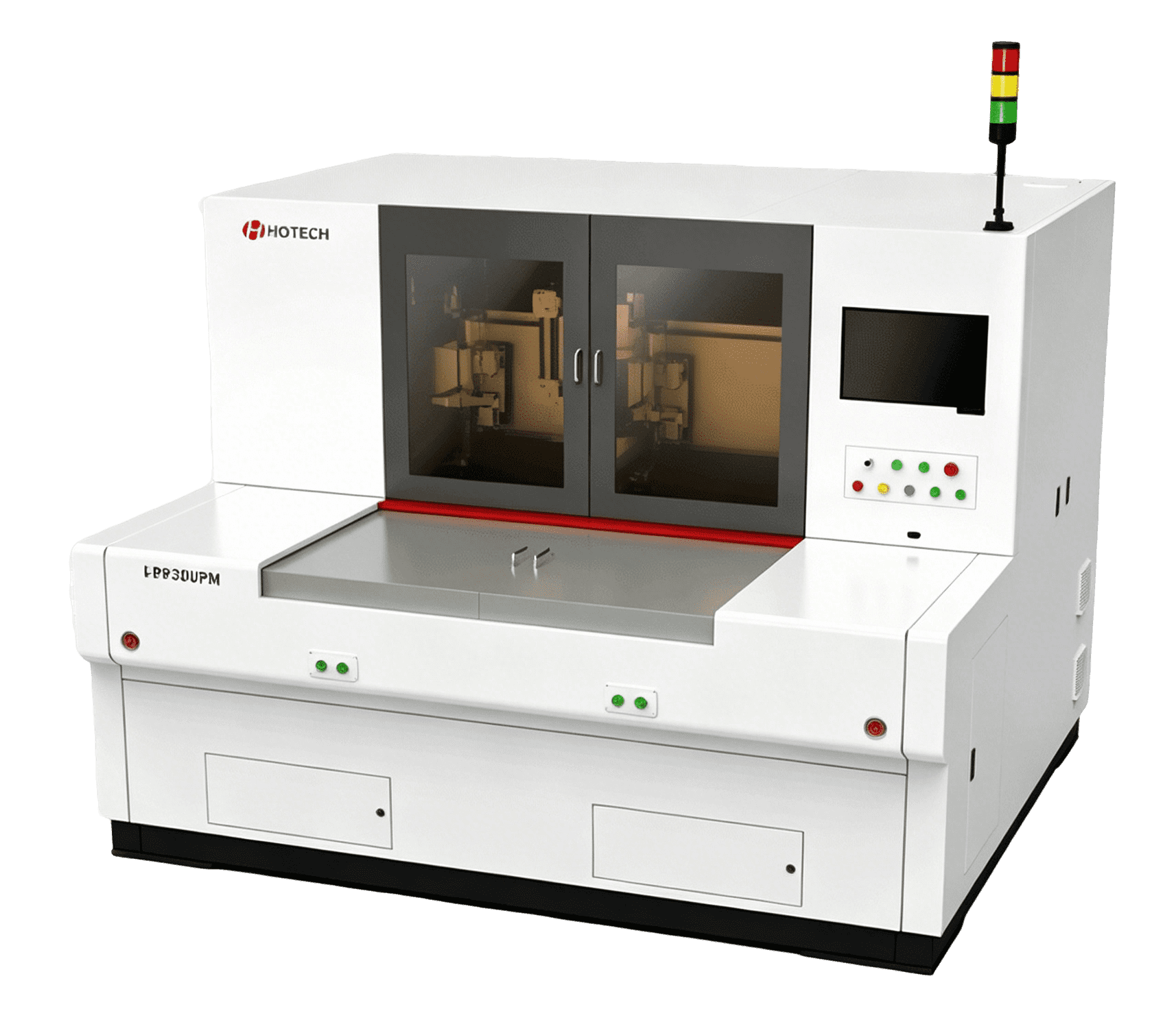
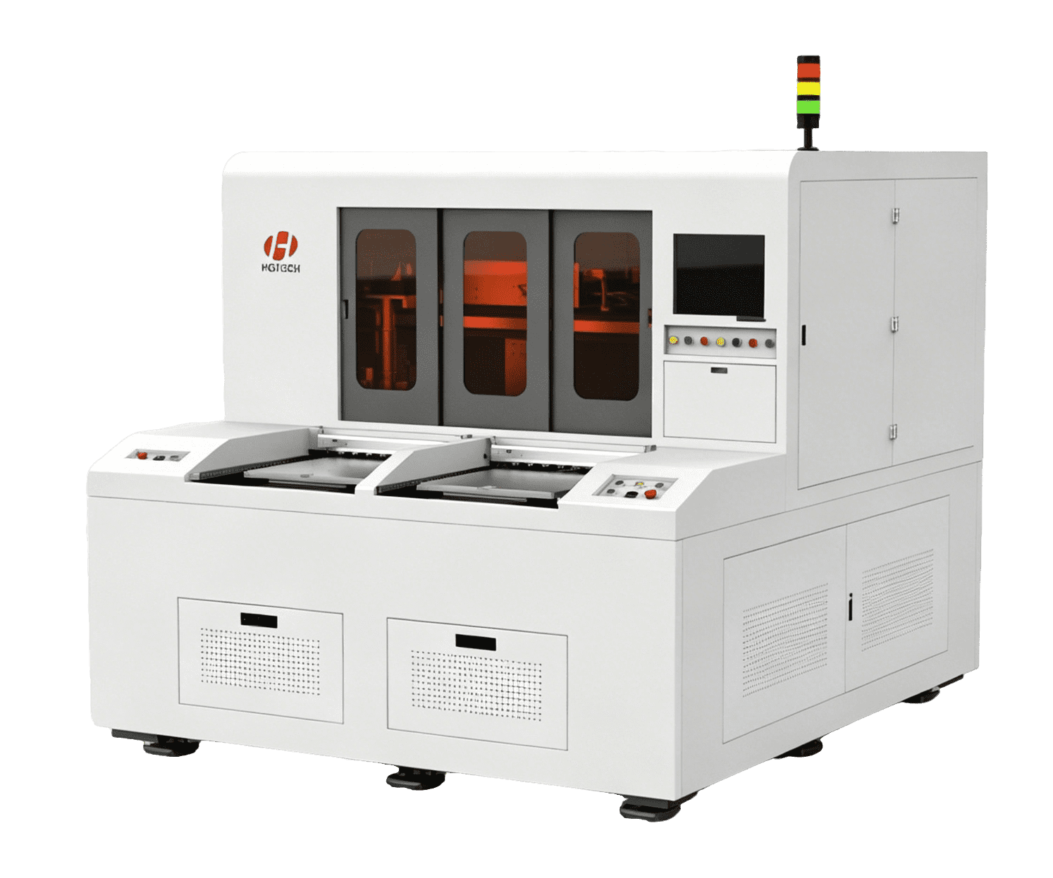
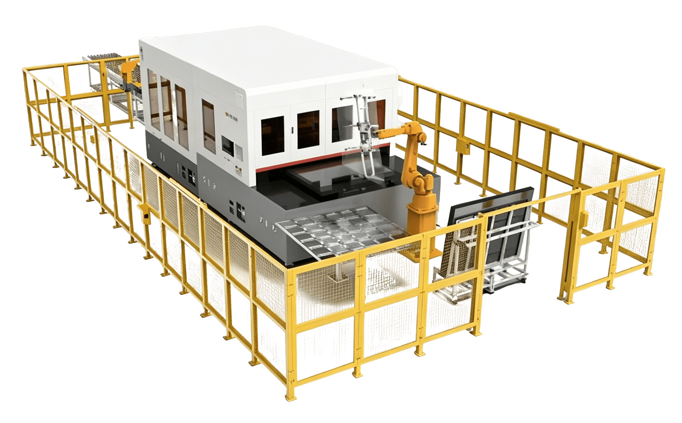
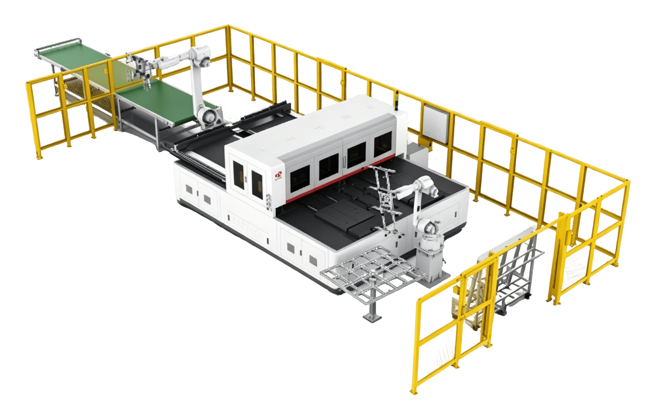
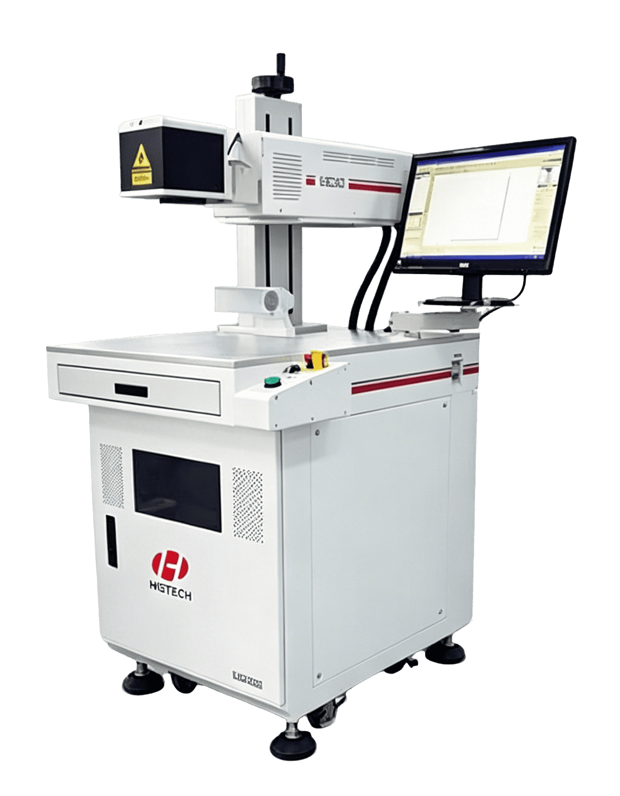
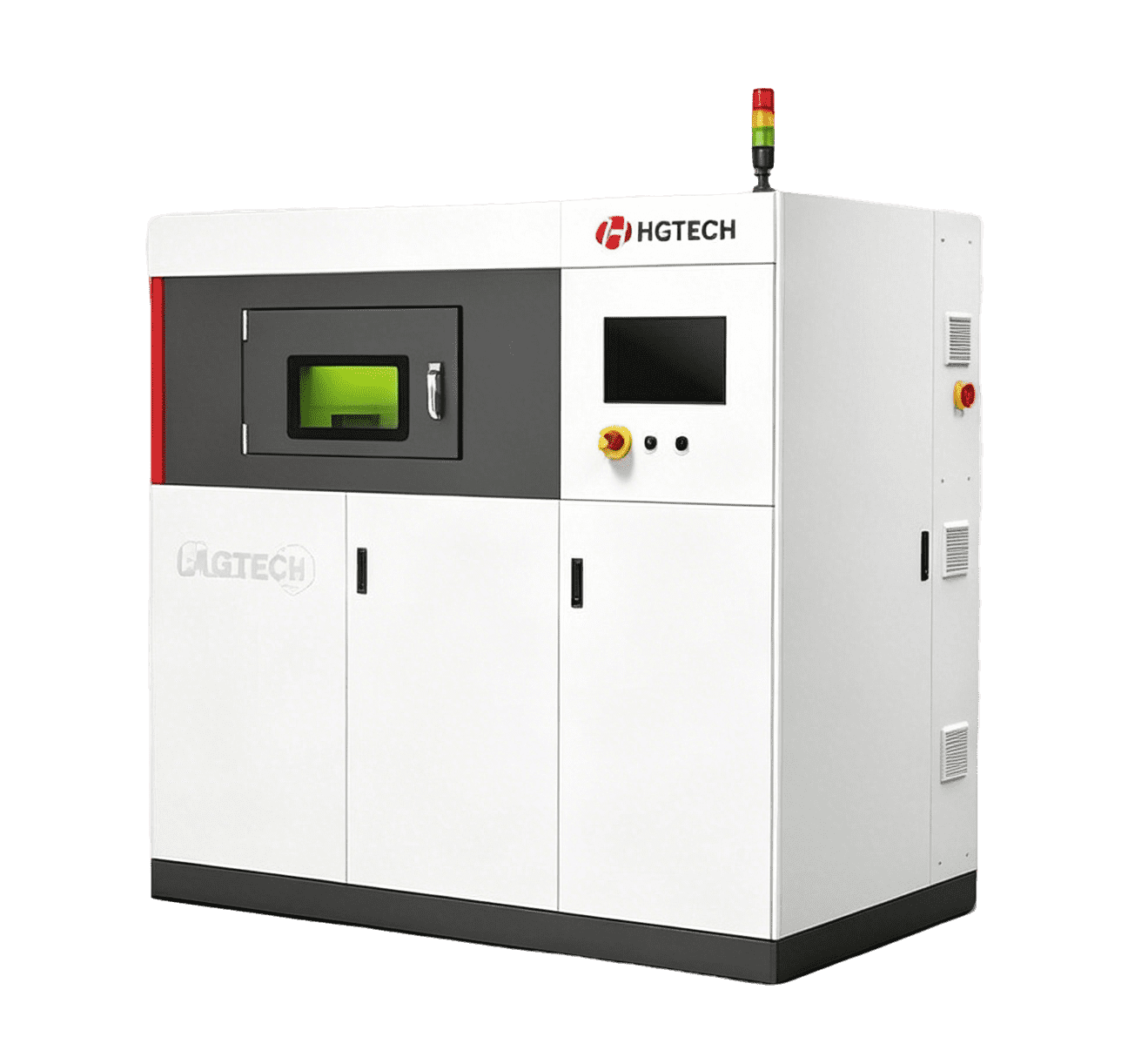
Semiconductor & Brittle Materials Industry

Precision laser and inspection solutions for semiconductor and brittle materials

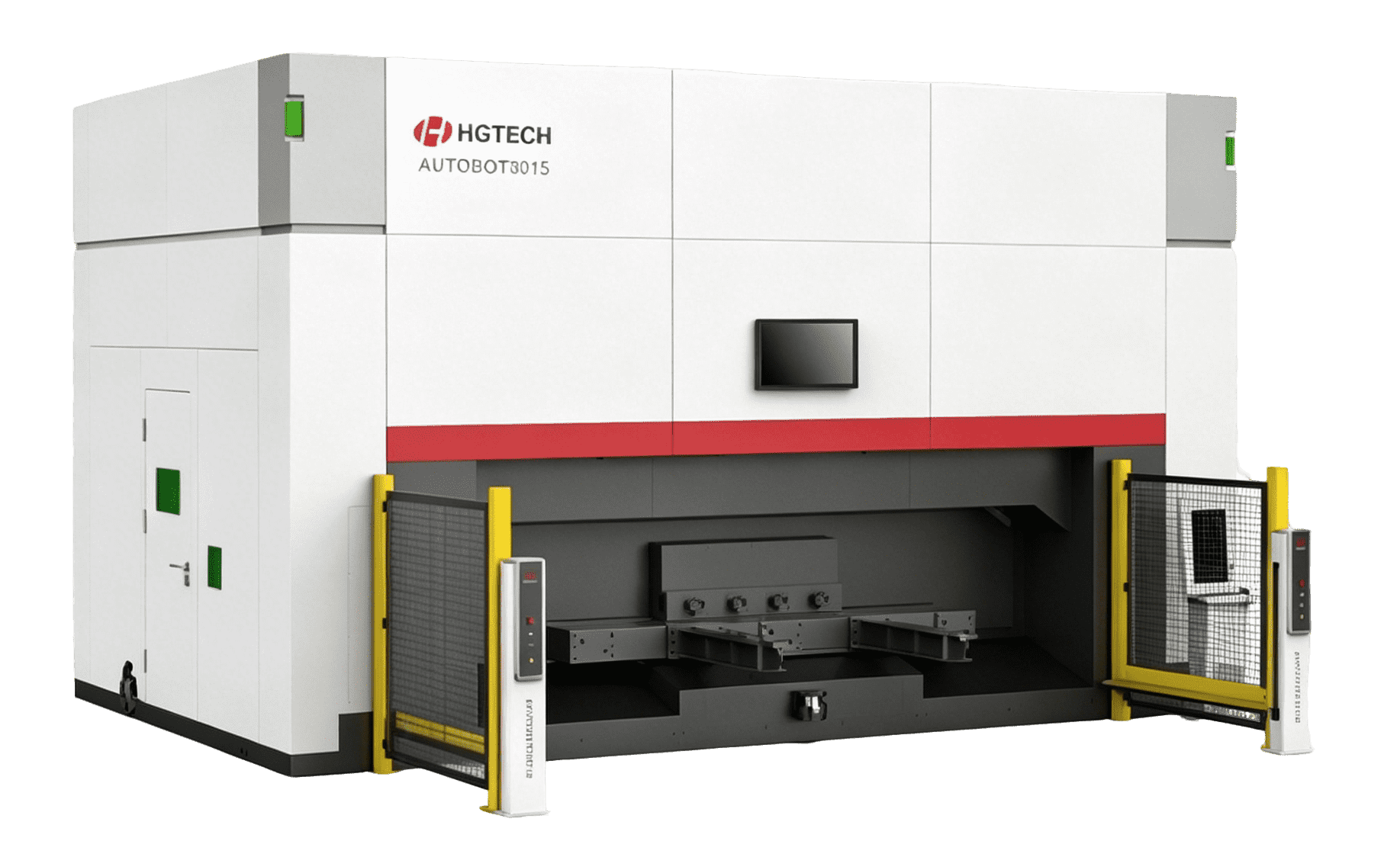
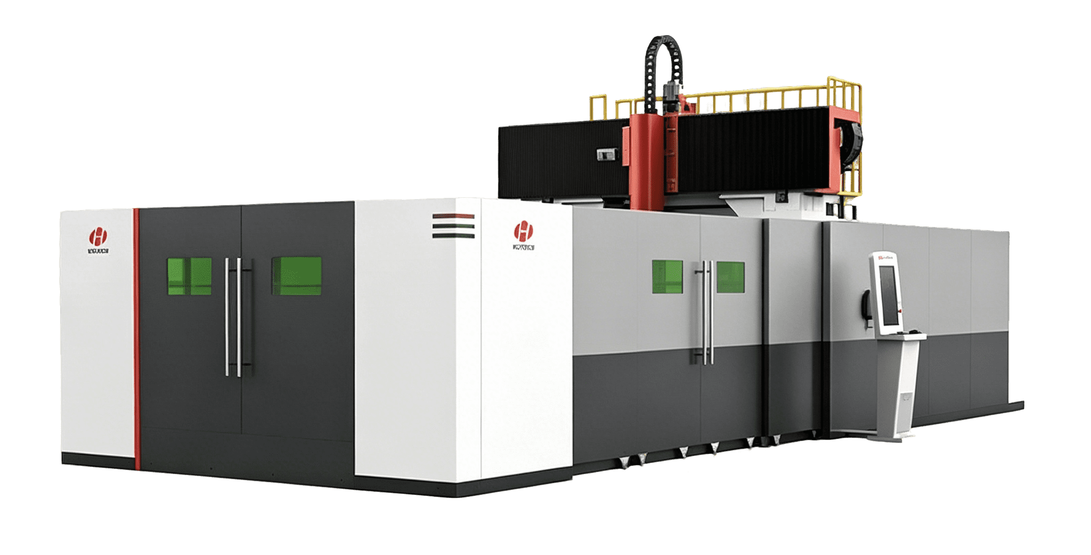
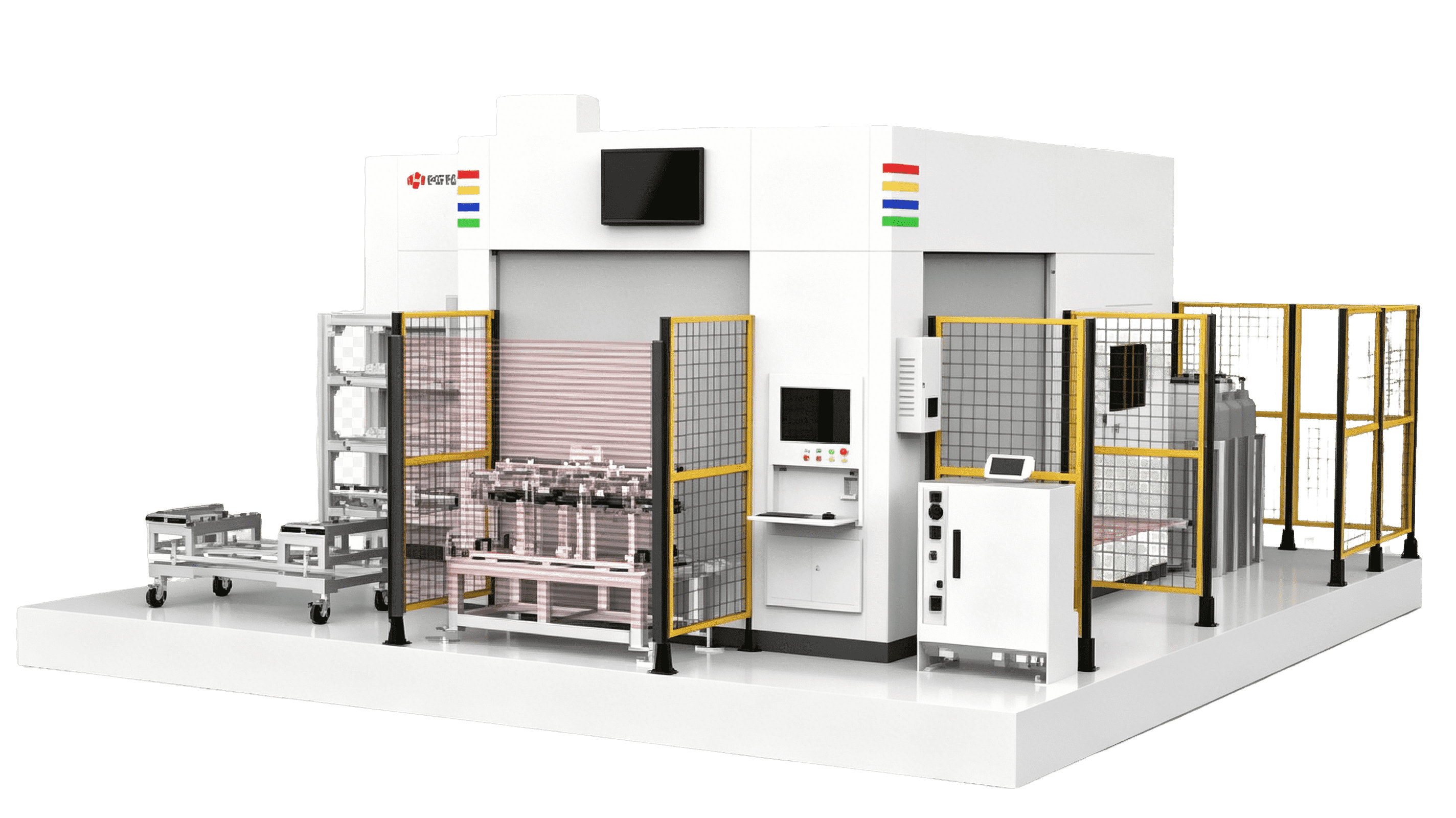
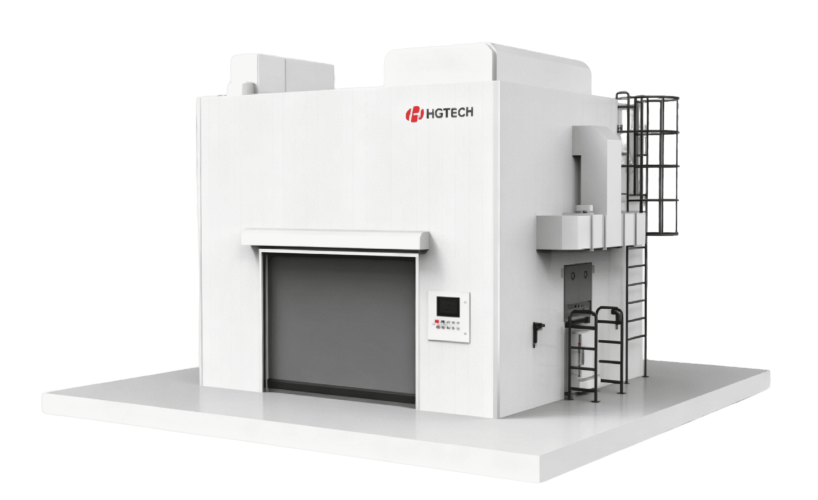
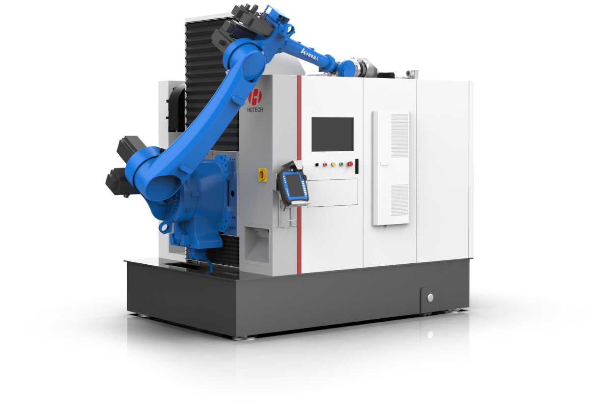
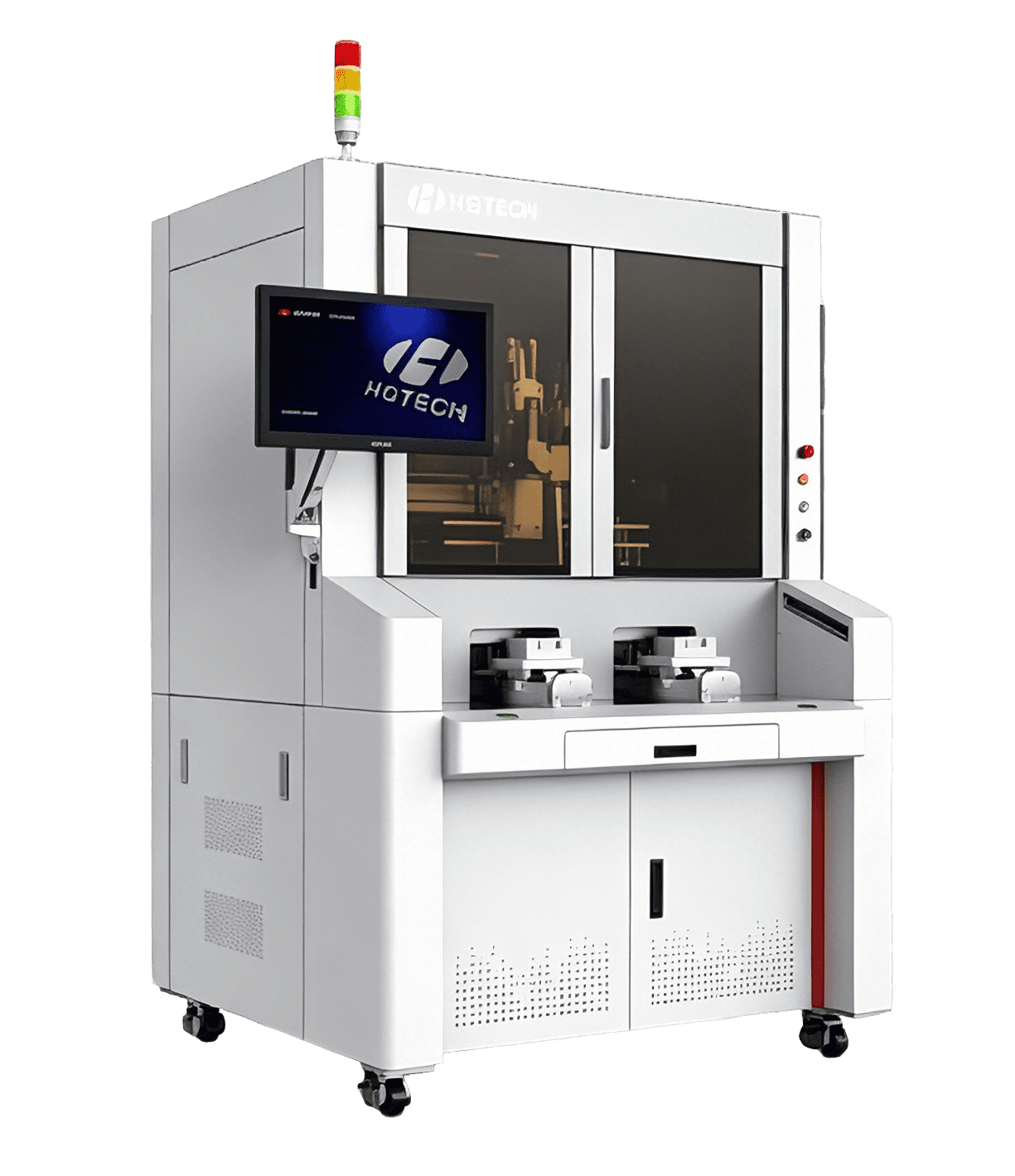
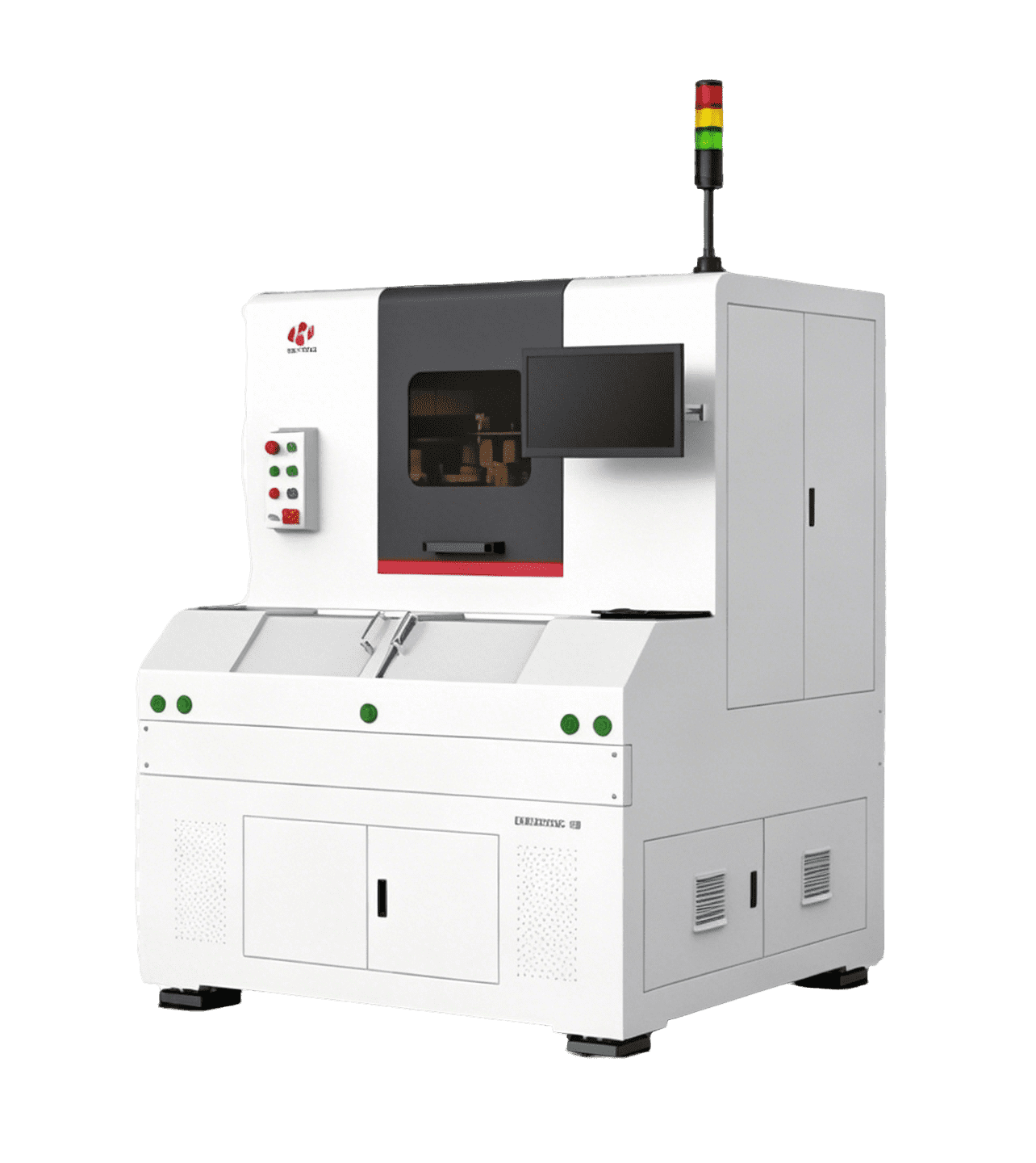
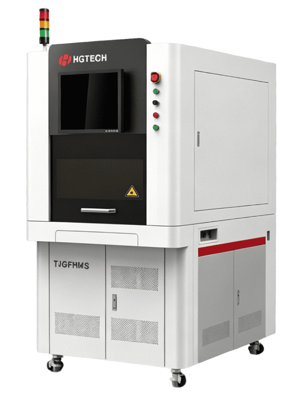
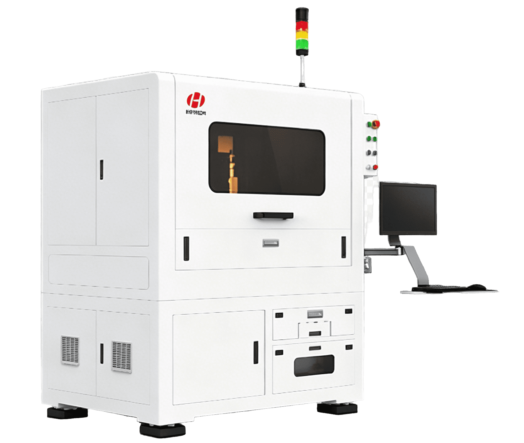
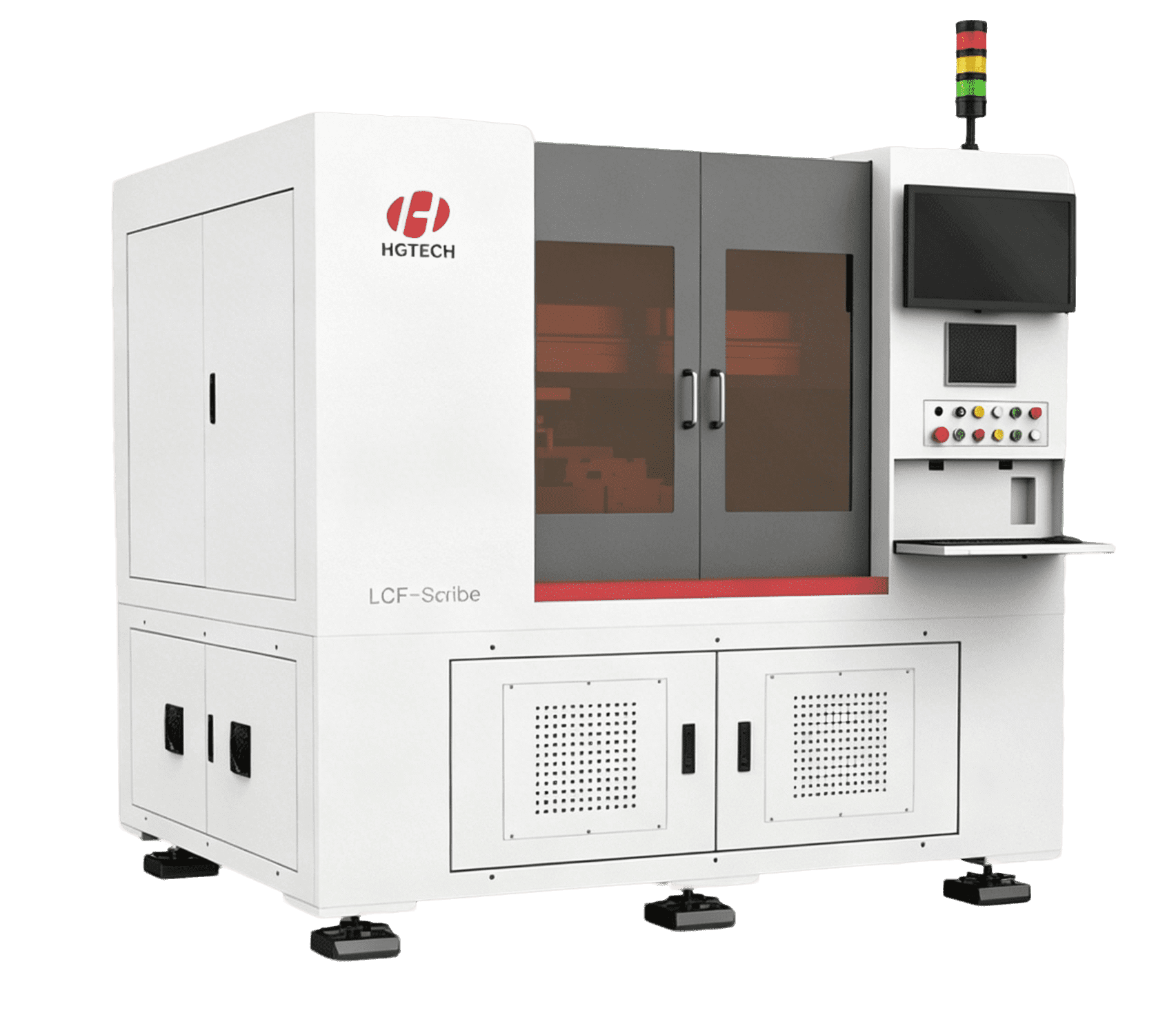
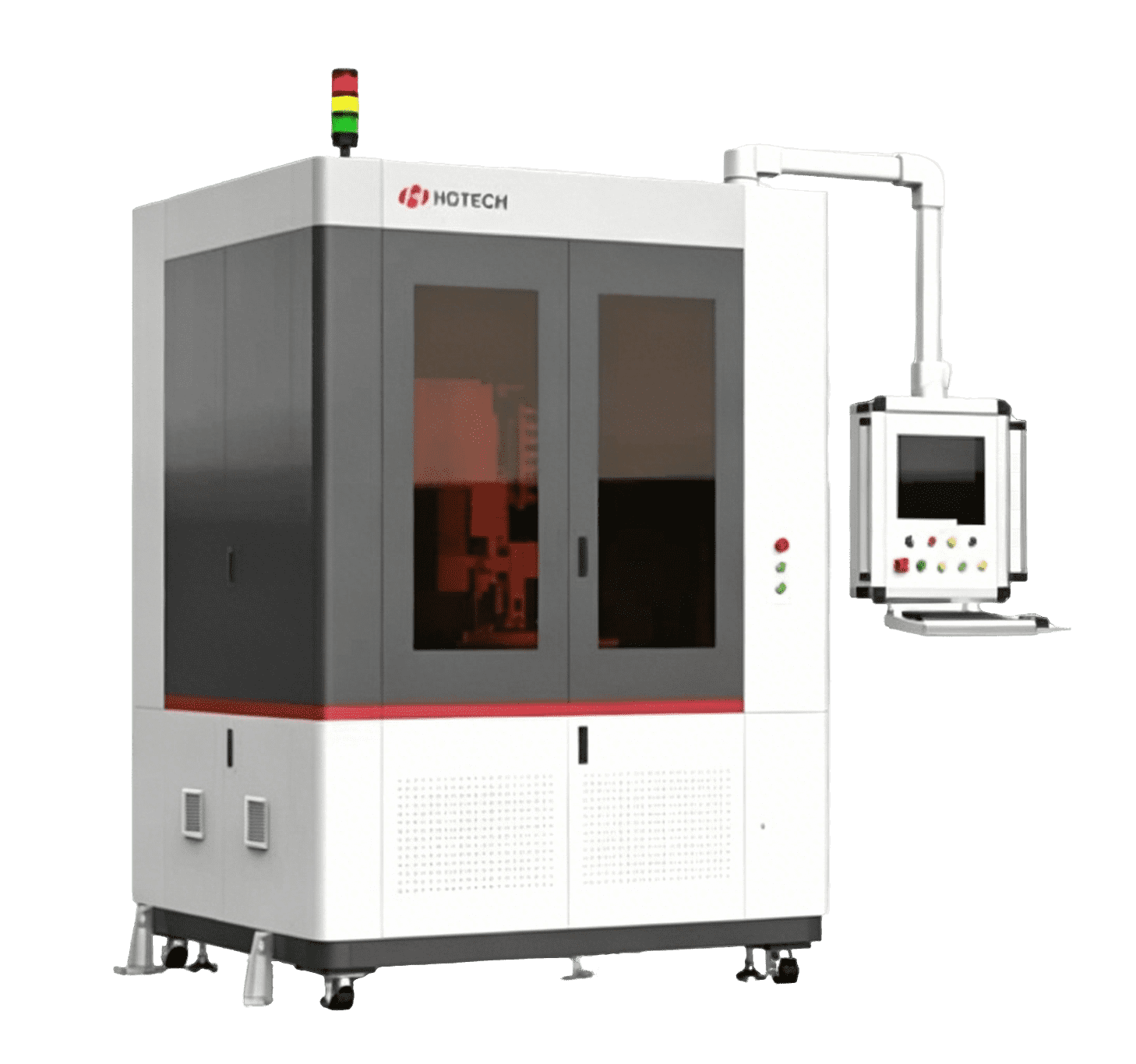
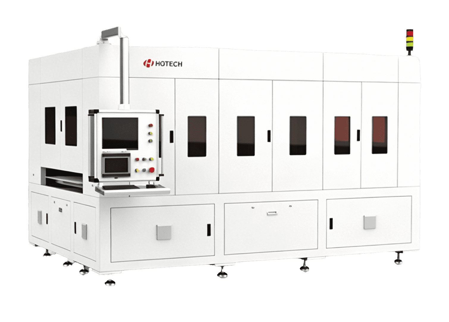
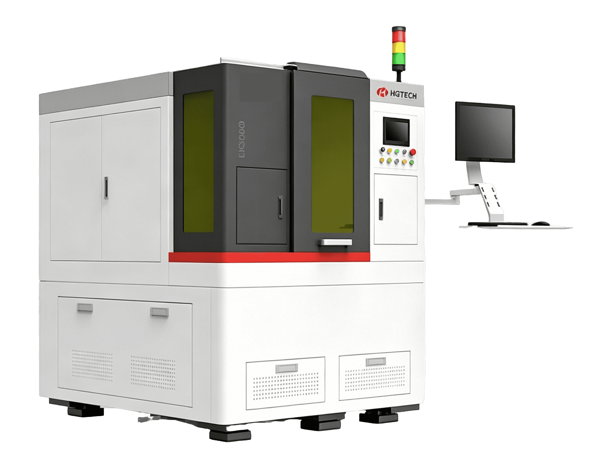
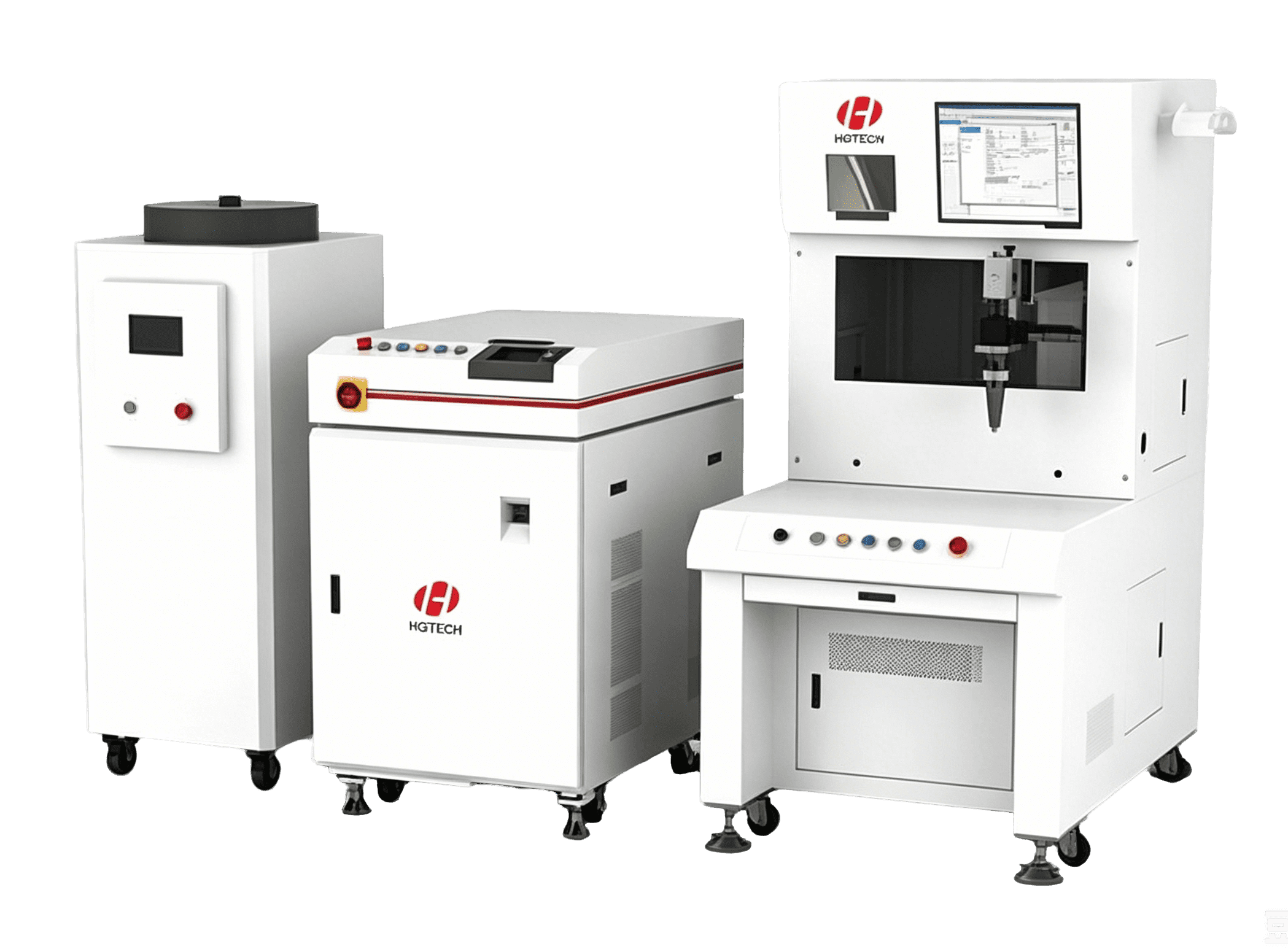
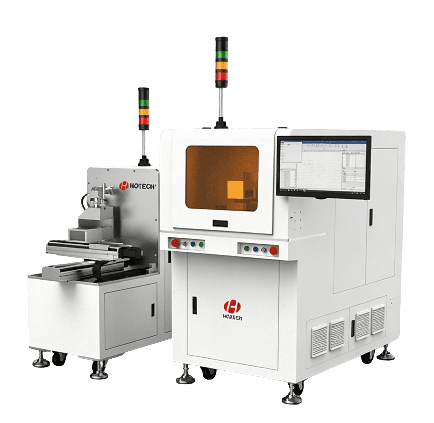
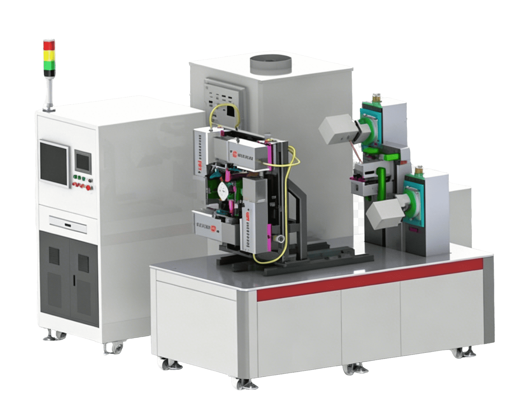
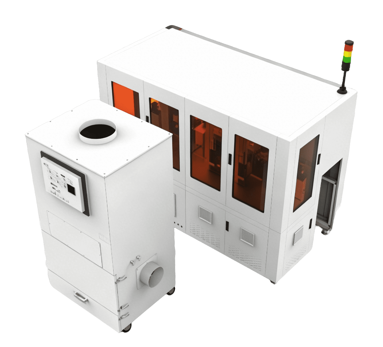
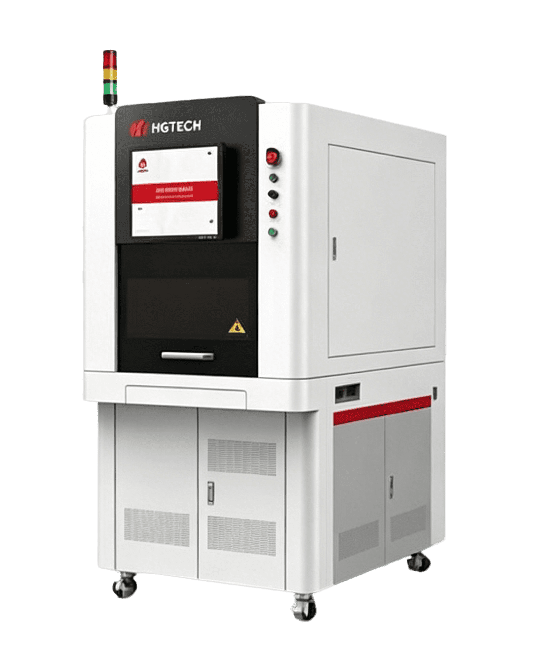
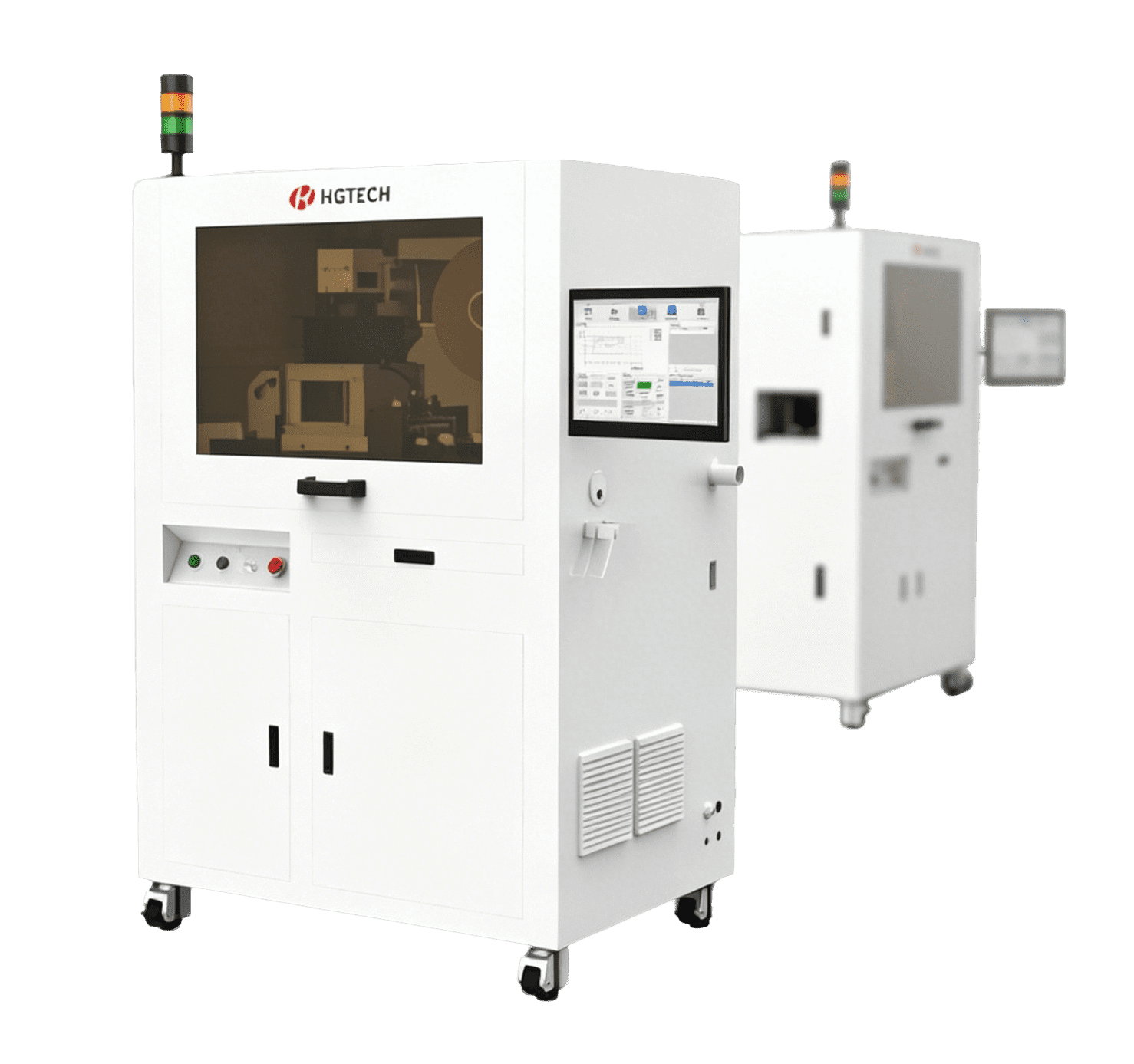
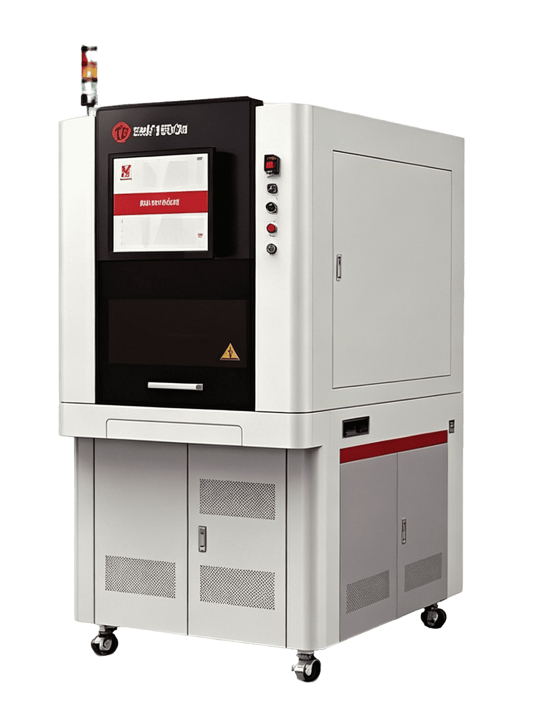
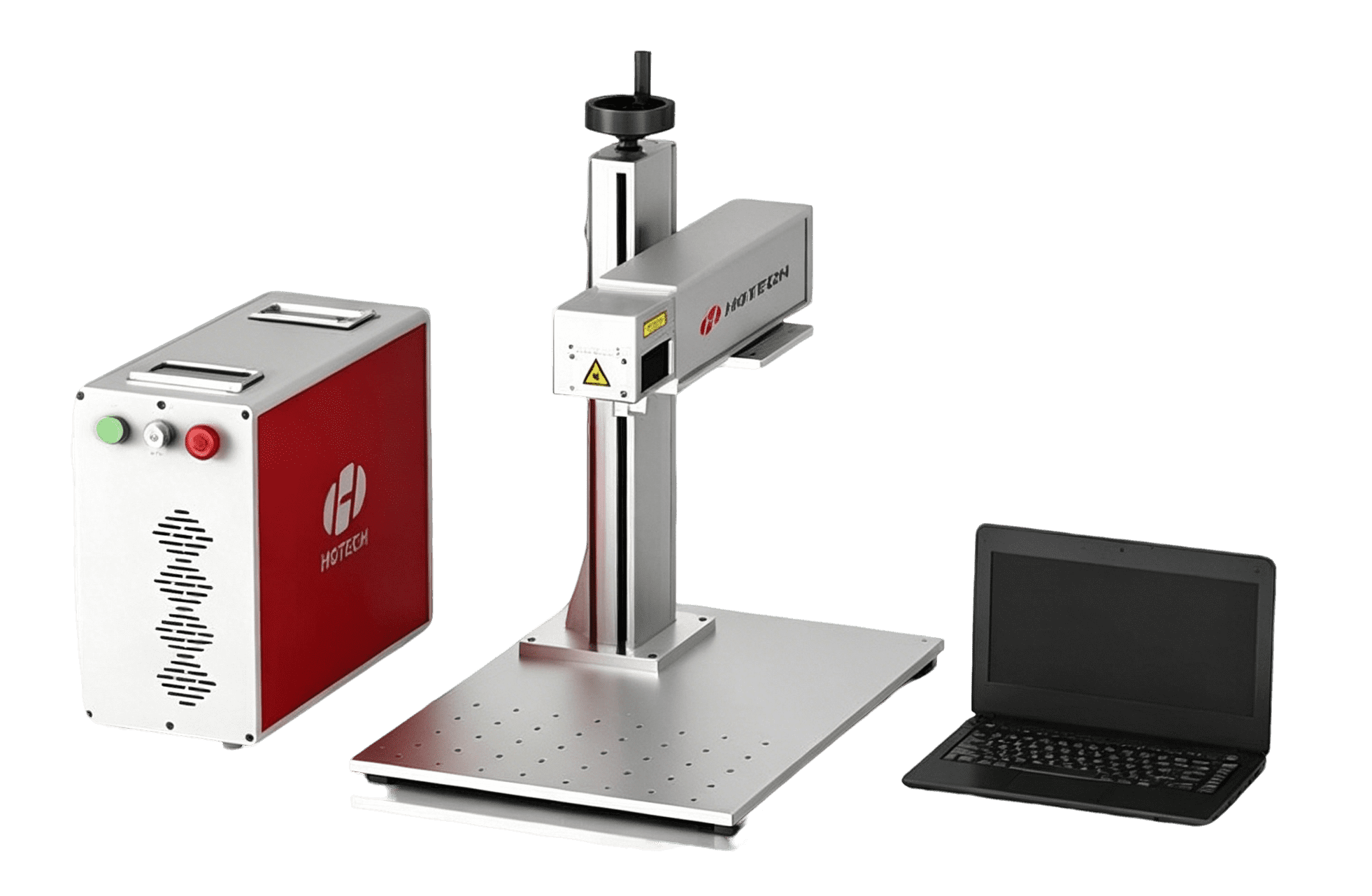
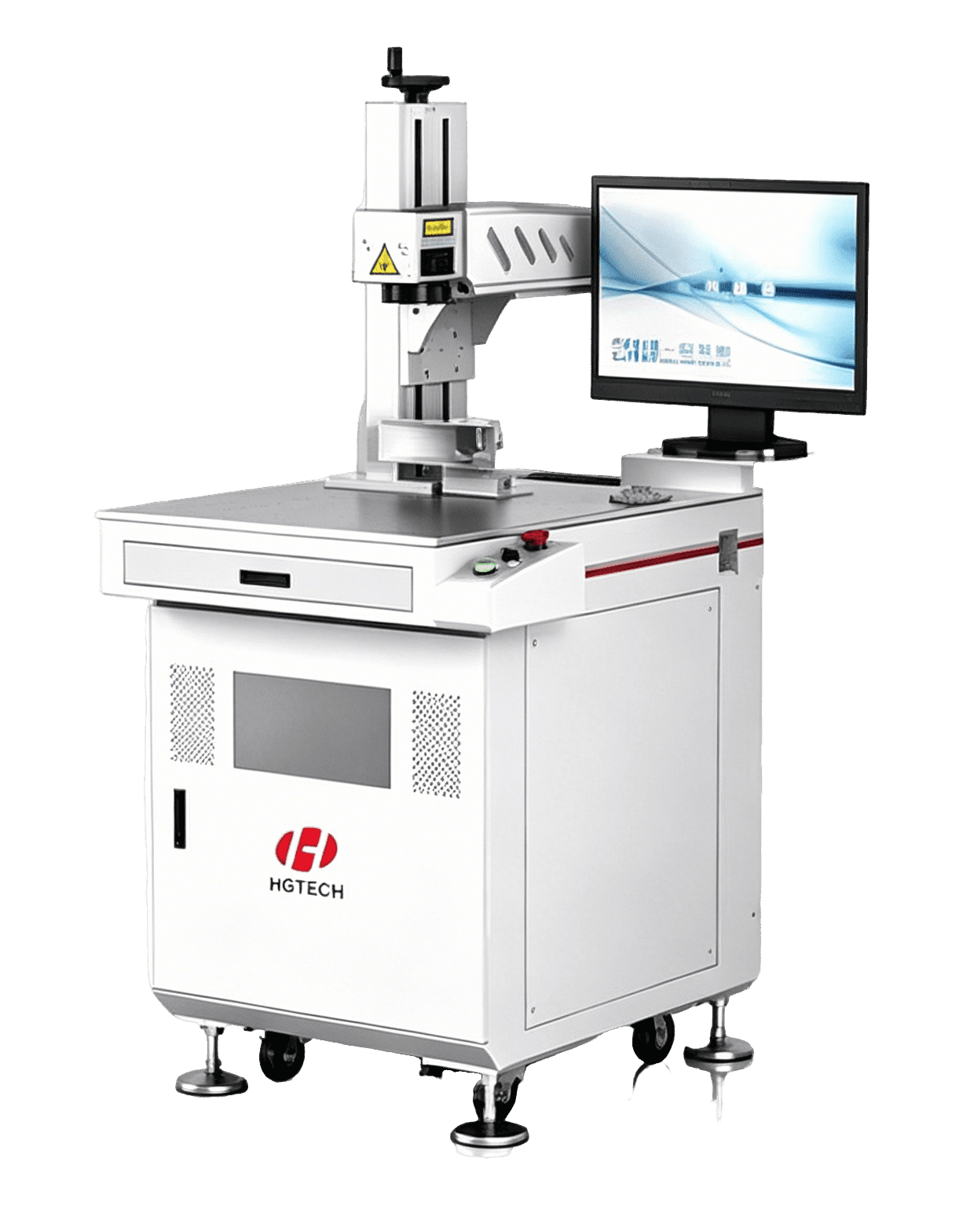
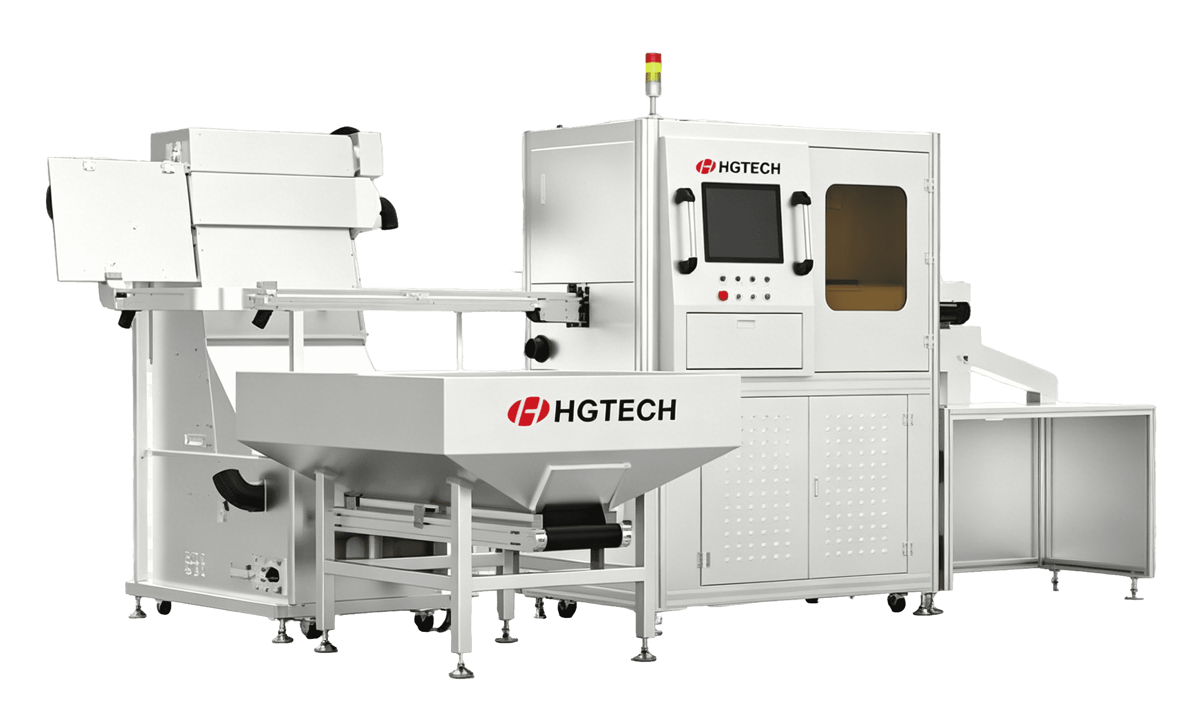
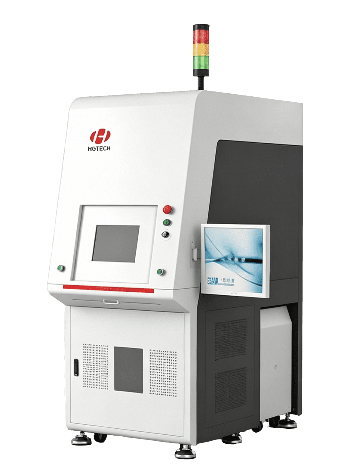
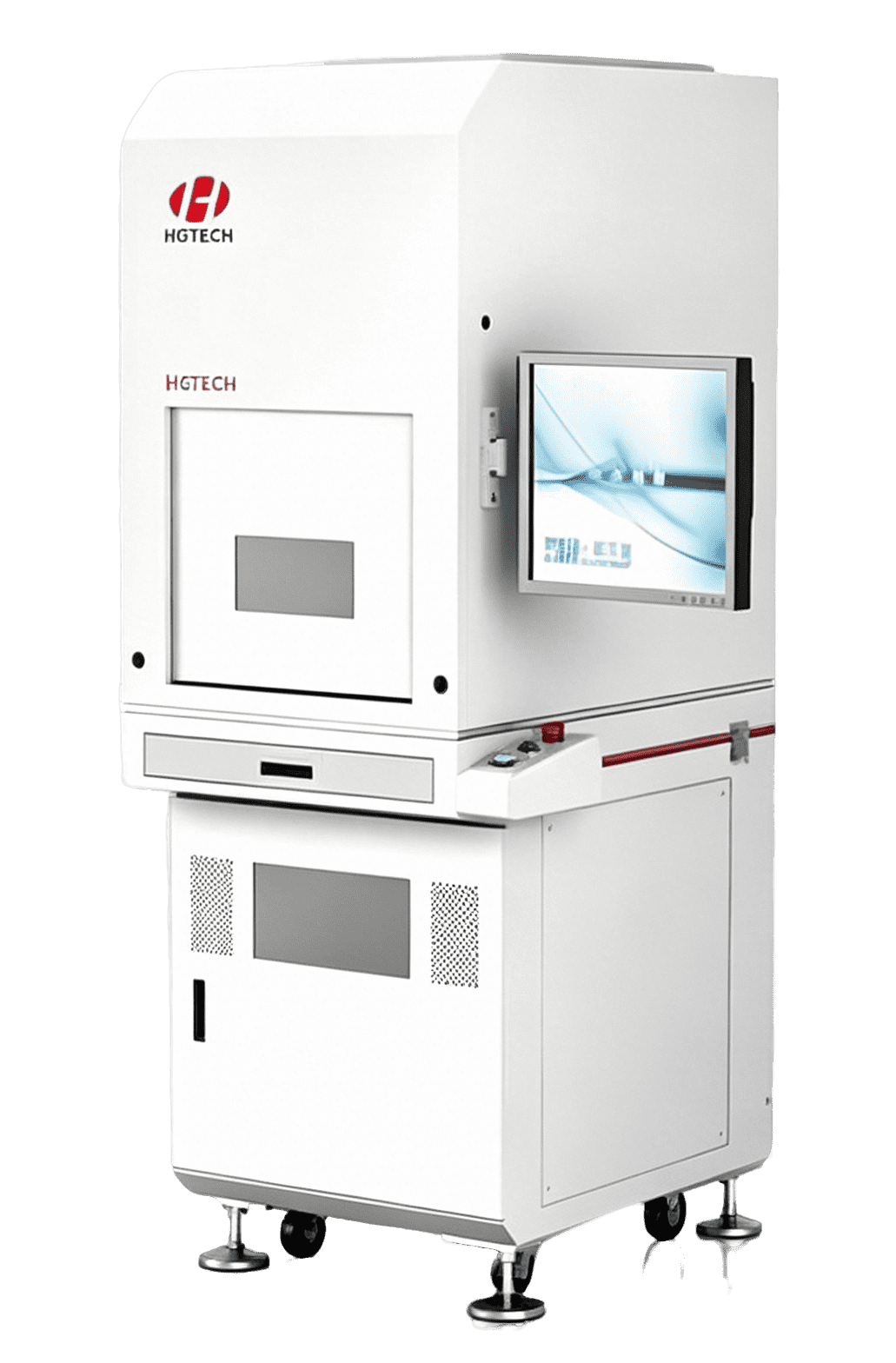
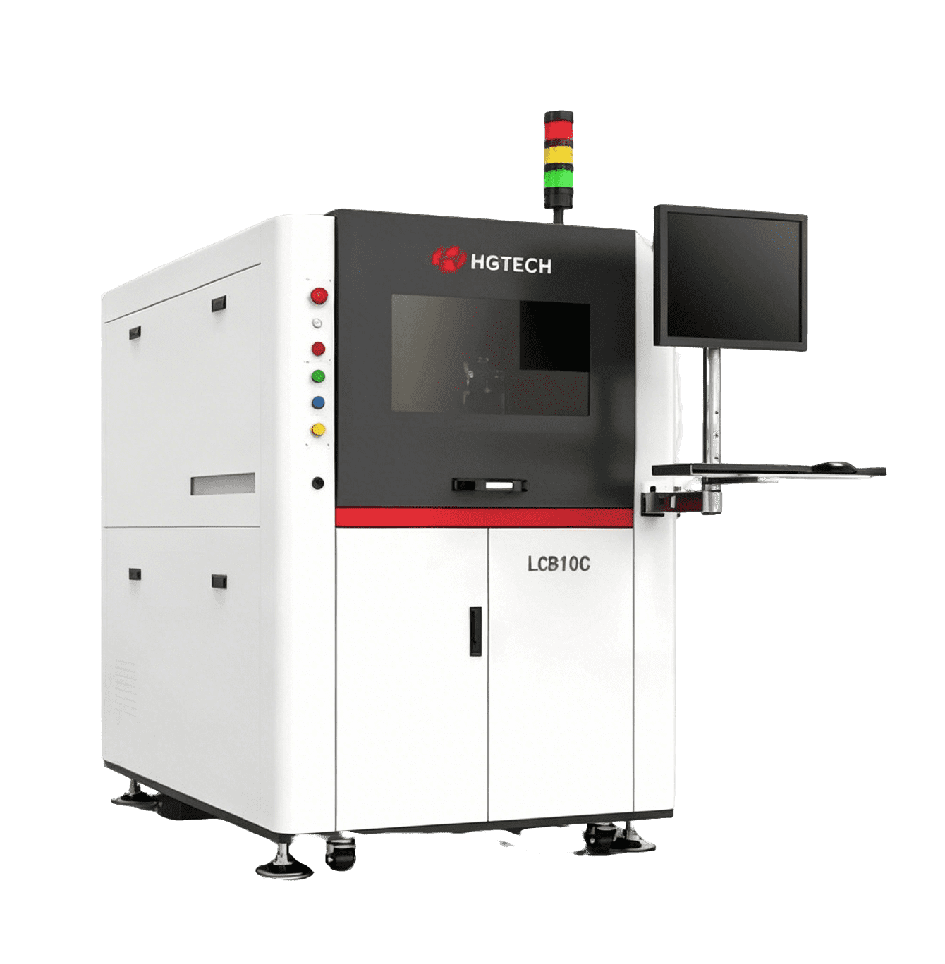
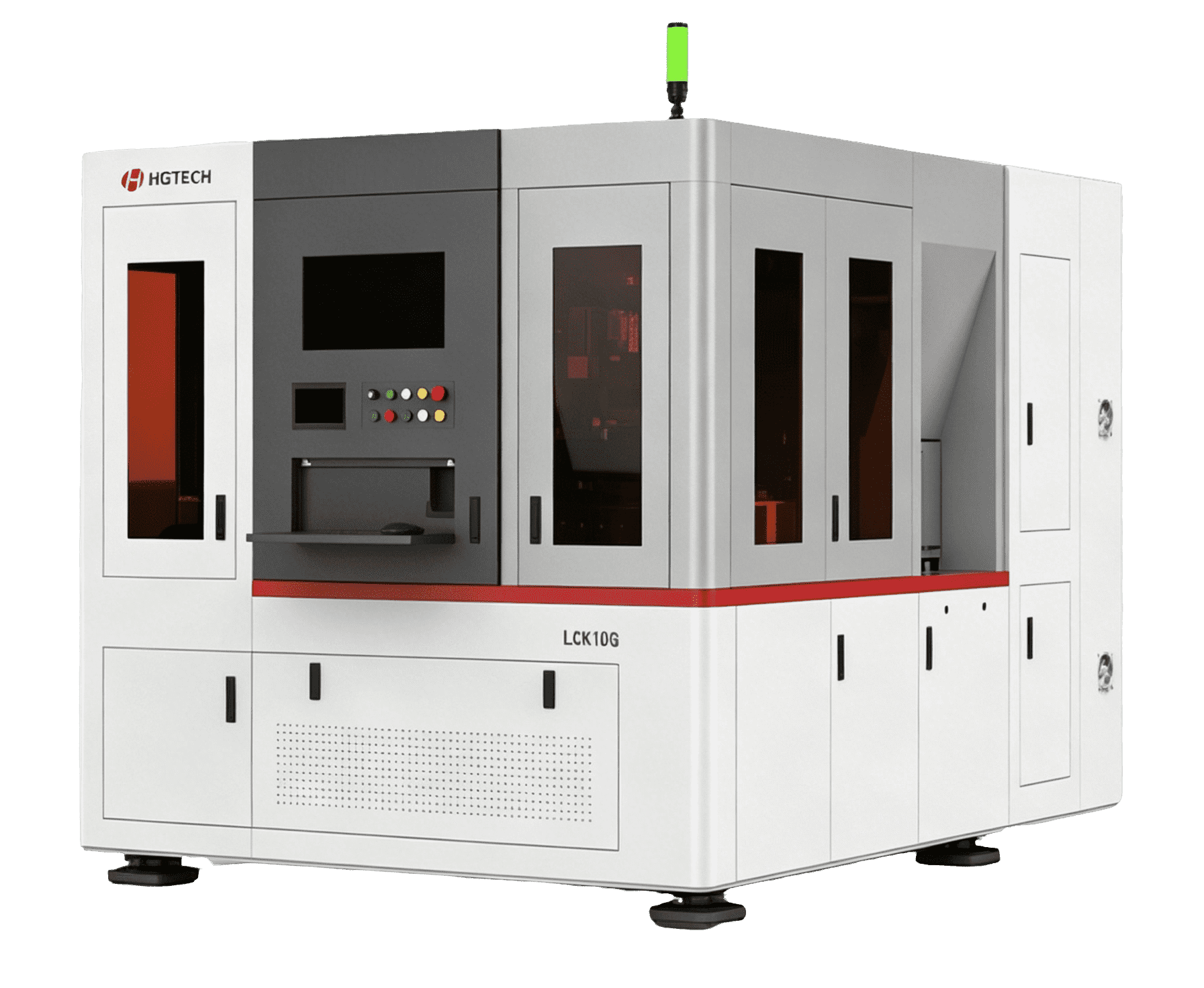
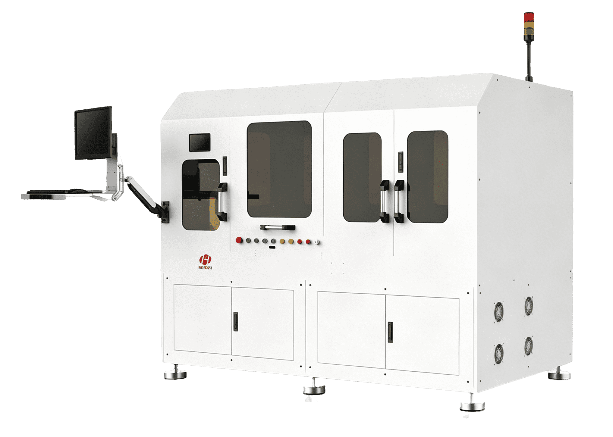
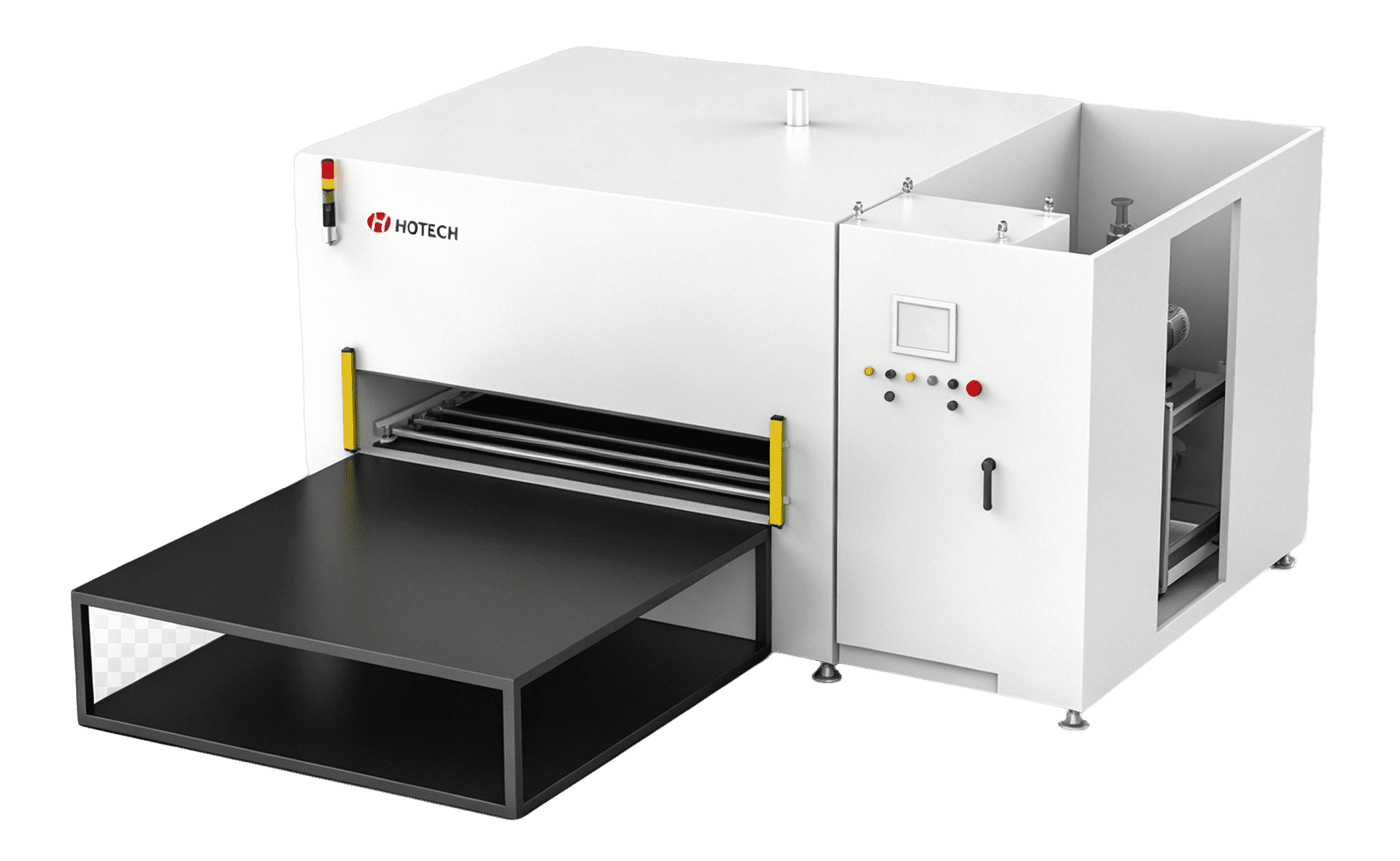
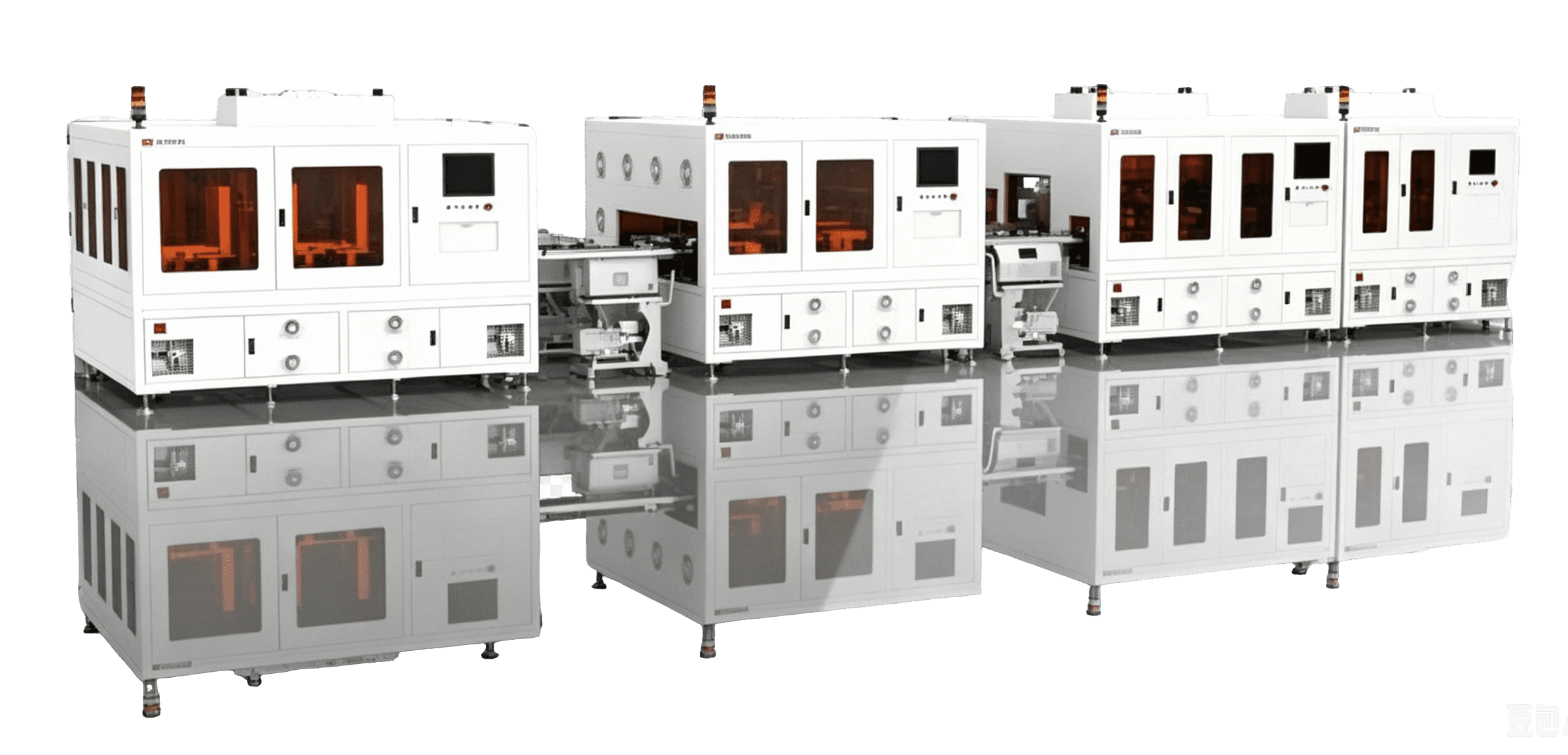
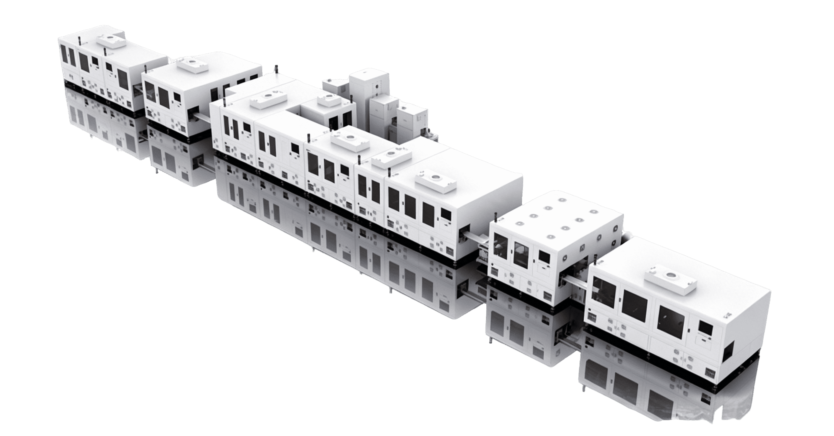
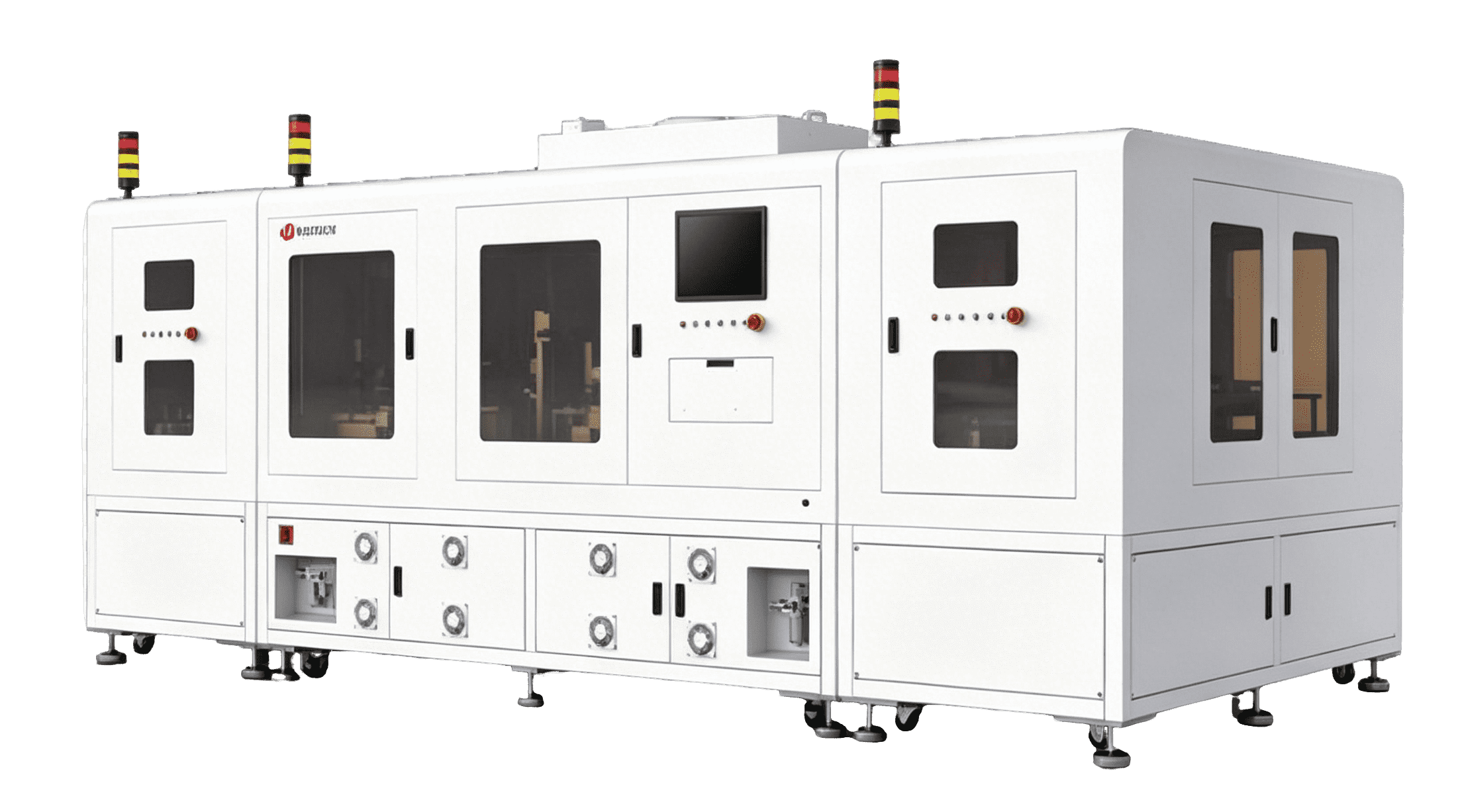
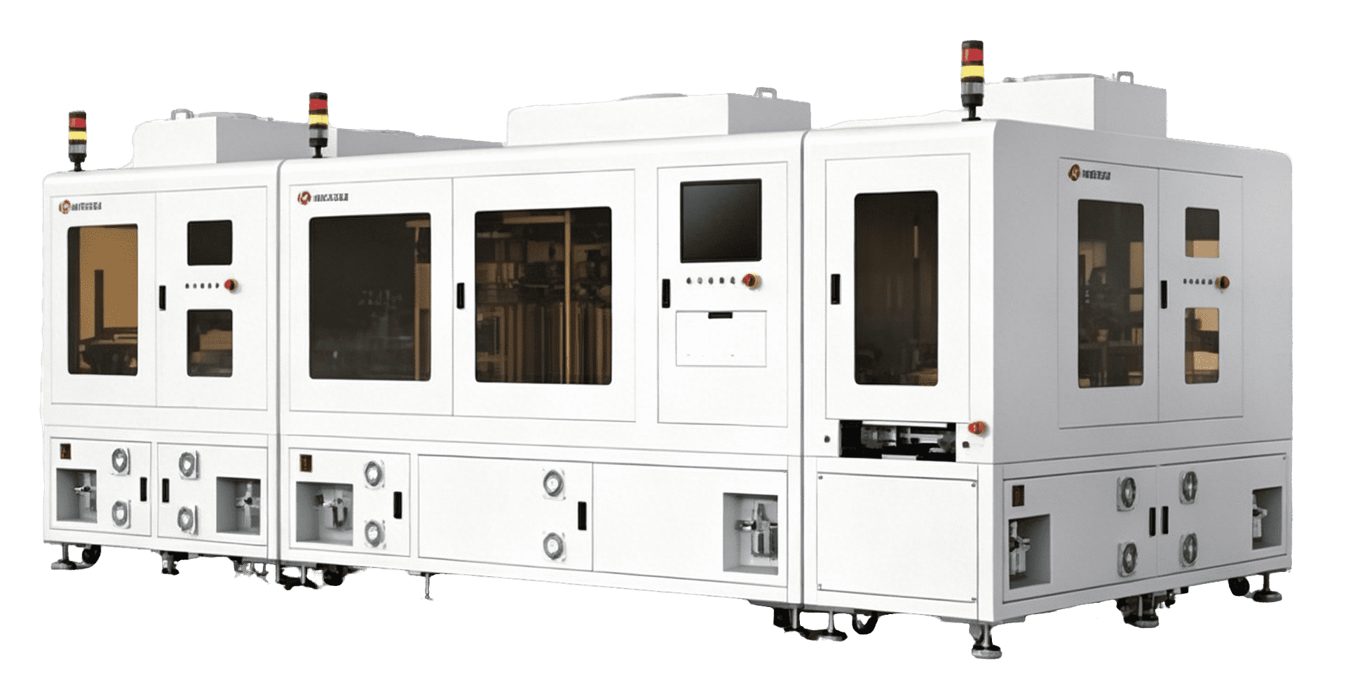
HGTECH provides semiconductor and brittle-material solutions covering wafer annealing, laser modification cutting, slotting, scribing, marking, defect detection, thickness measurement, and precision glass or ceramic processing.

  • 01

    Wafer Annealing

    Backside metal annealing for SiC wafer device performance.
  • 02

    Wafer Cutting & Dicing

    Modified cutting, stealth dicing, slotting, and scribing for semiconductor wafers.
  • 03

    Wafer Marking

    Fully Automated Wafer Marking for identification and traceability.
  • 04

    Inspection & Measurement

    Defect detection and thickness measurement for wafers, substrates, and epitaxial wafers.
  • 05

    Hard and Brittle Materials Processing

    Glass, quartz, optical glass, ceramic substrate, and other hard and brittle material cutting or drilling.
  • 06

    Manufacturing Support
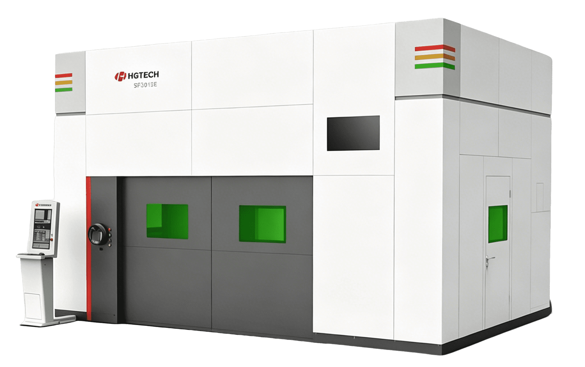
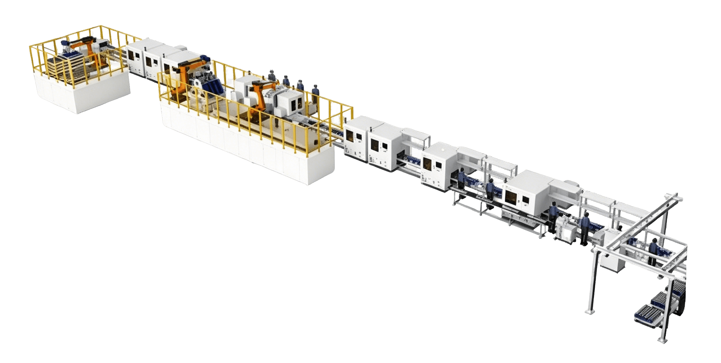
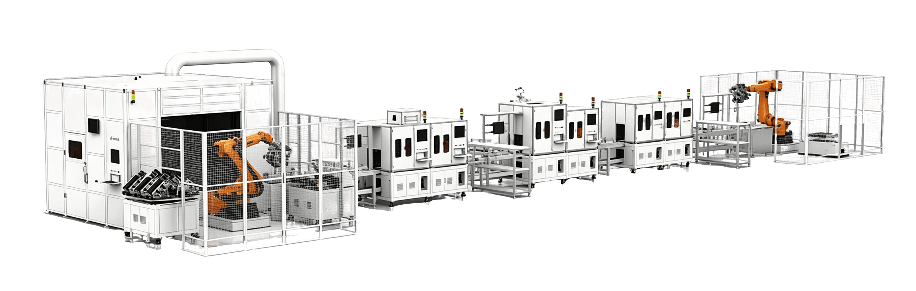
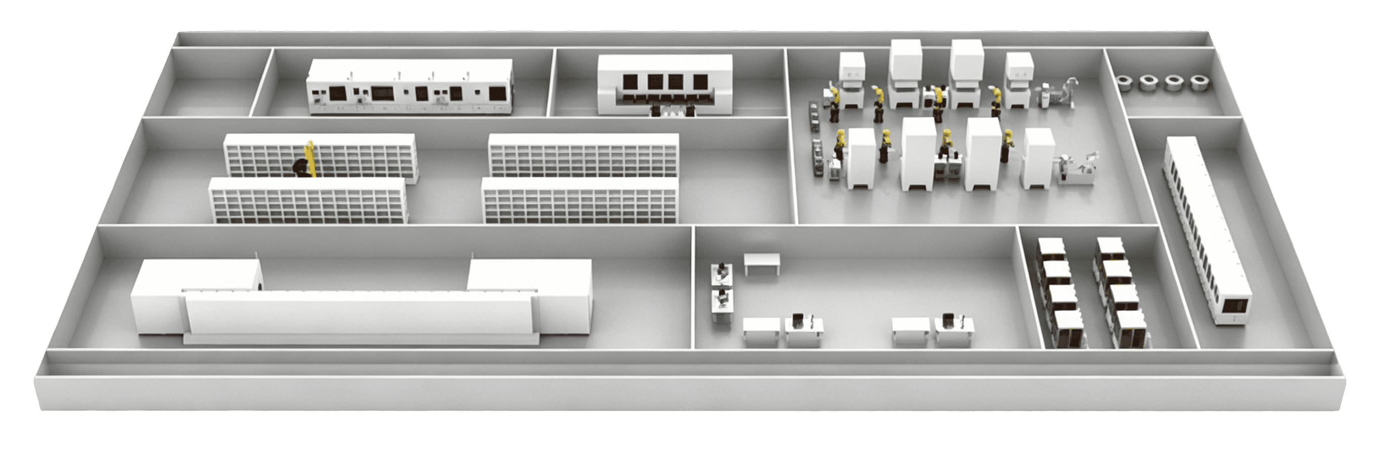
    Automation and smart factory support for semiconductor-related production.

Semiconductor

  • Wafer Laser Annealing

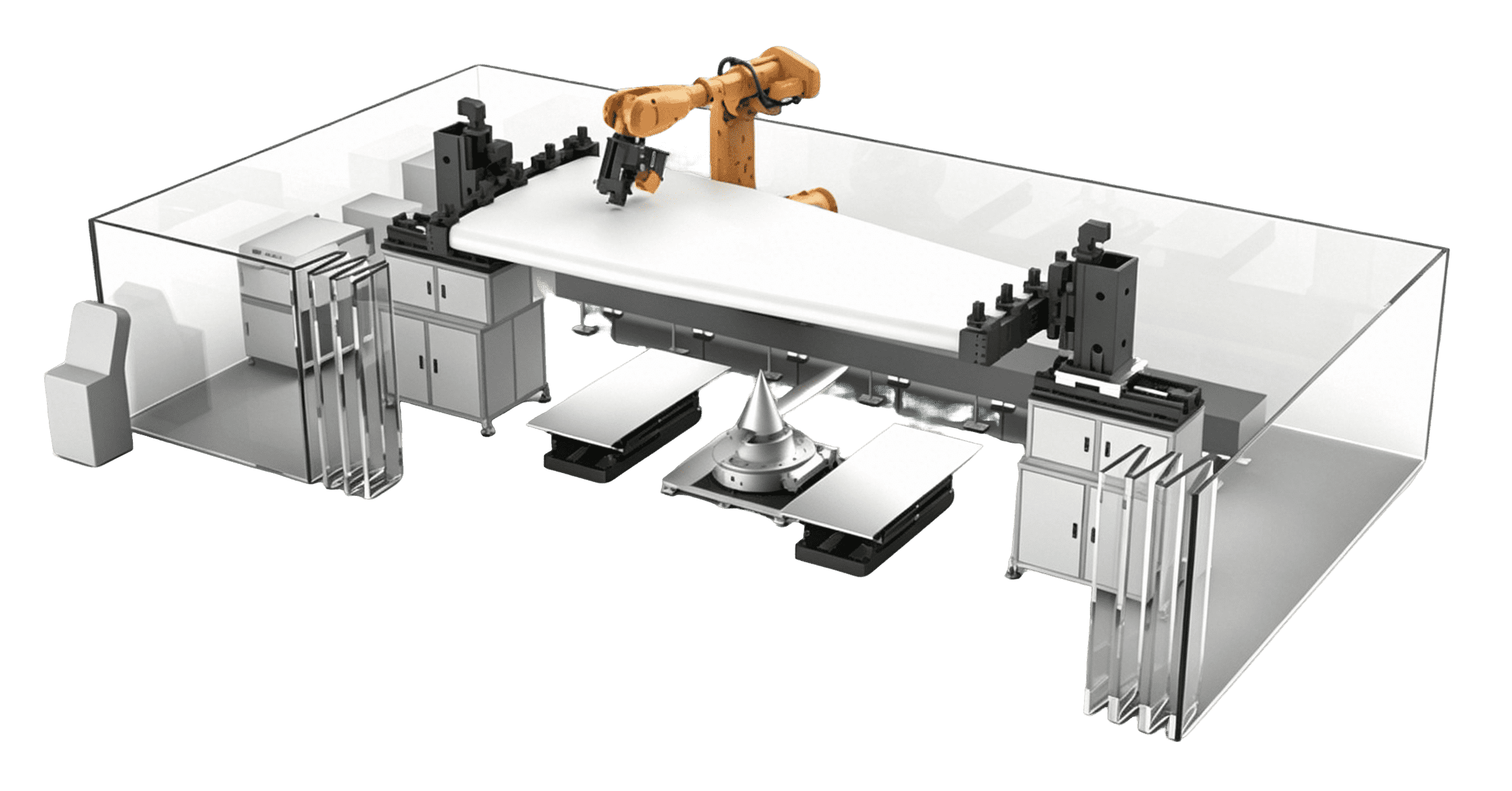
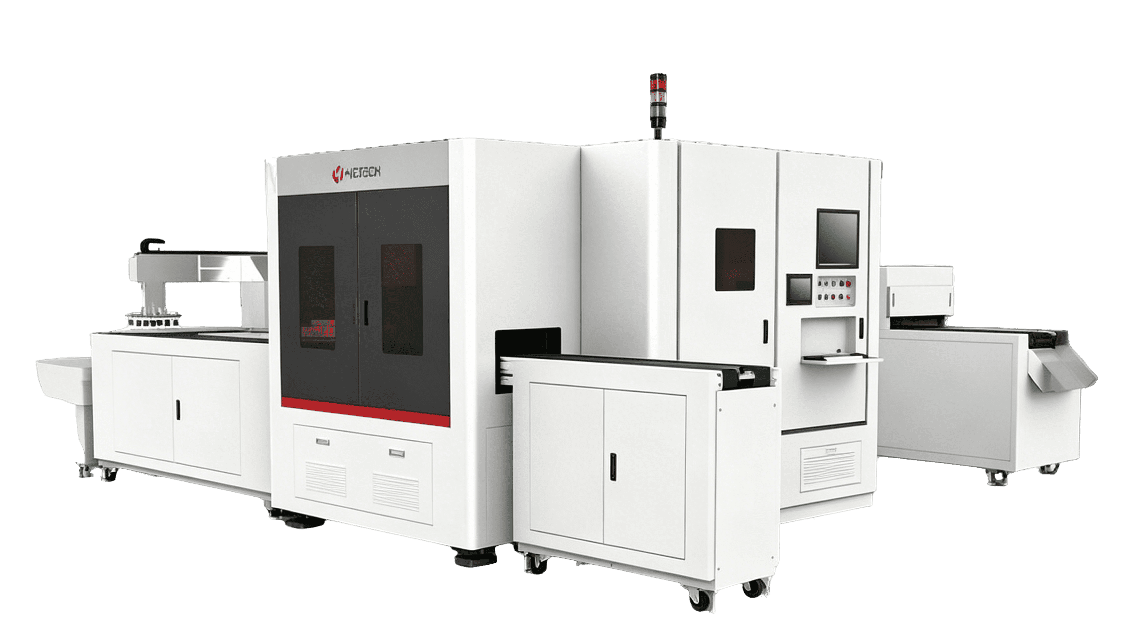
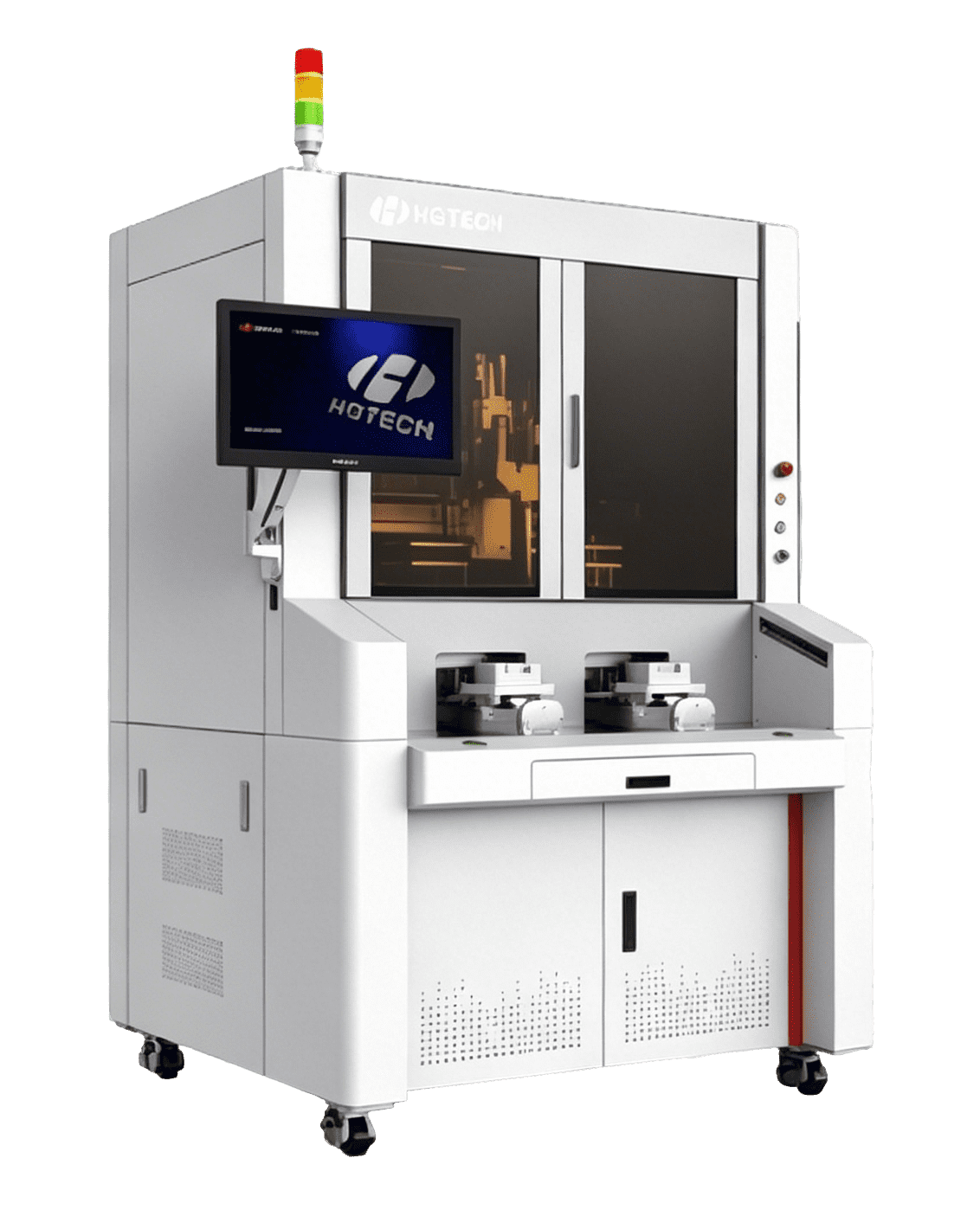
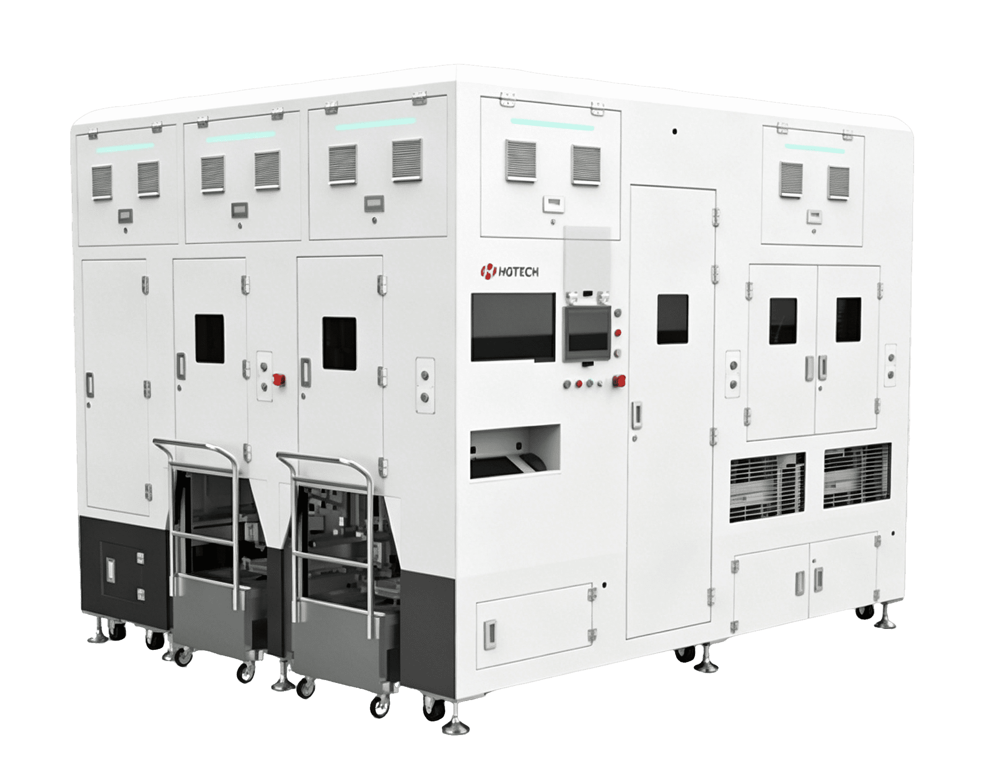
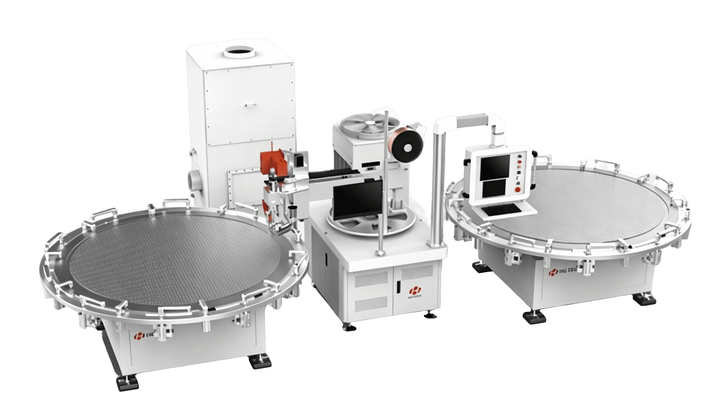
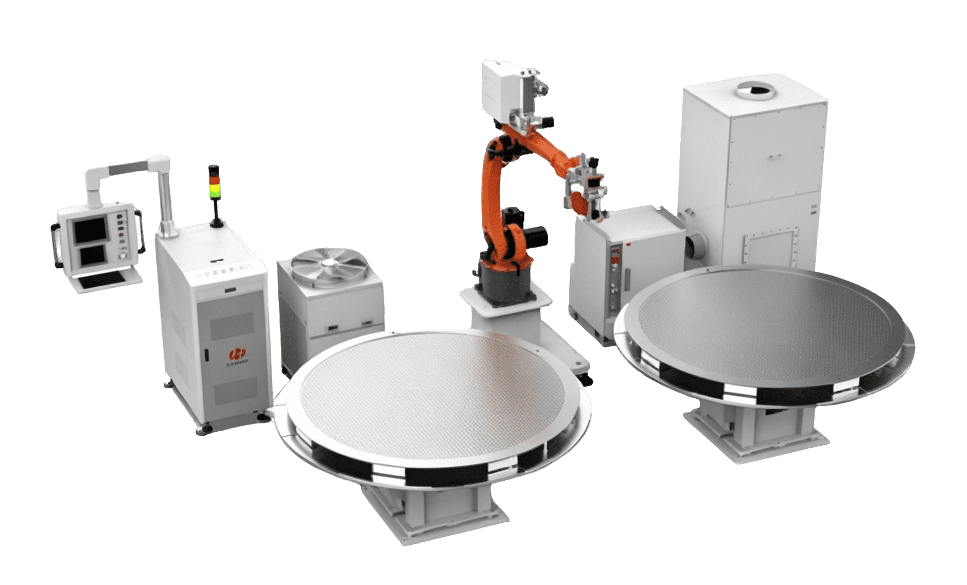
    Wafer laser annealing supports backside metal annealing for SiC wafers through coordinated wafer handling, laser annealing, and precision motion control.
    Value Points
    Supports SiC wafer backside metal annealing | Helps improve ohmic contact | Designed for fully automated wafer processing
    Recommended Products
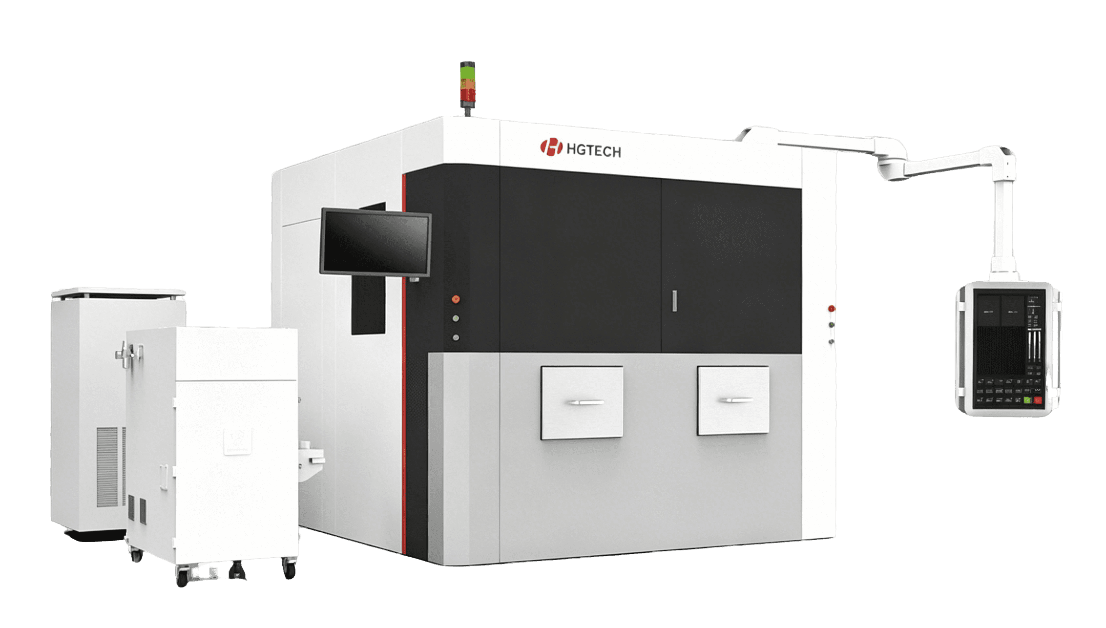
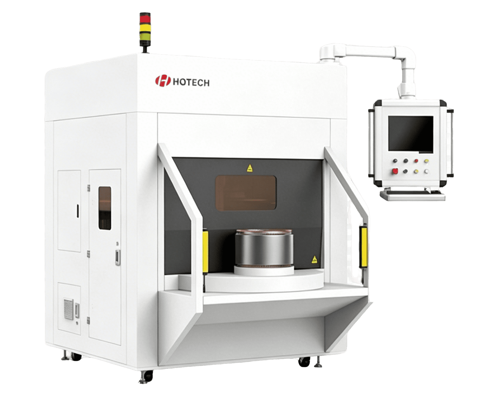
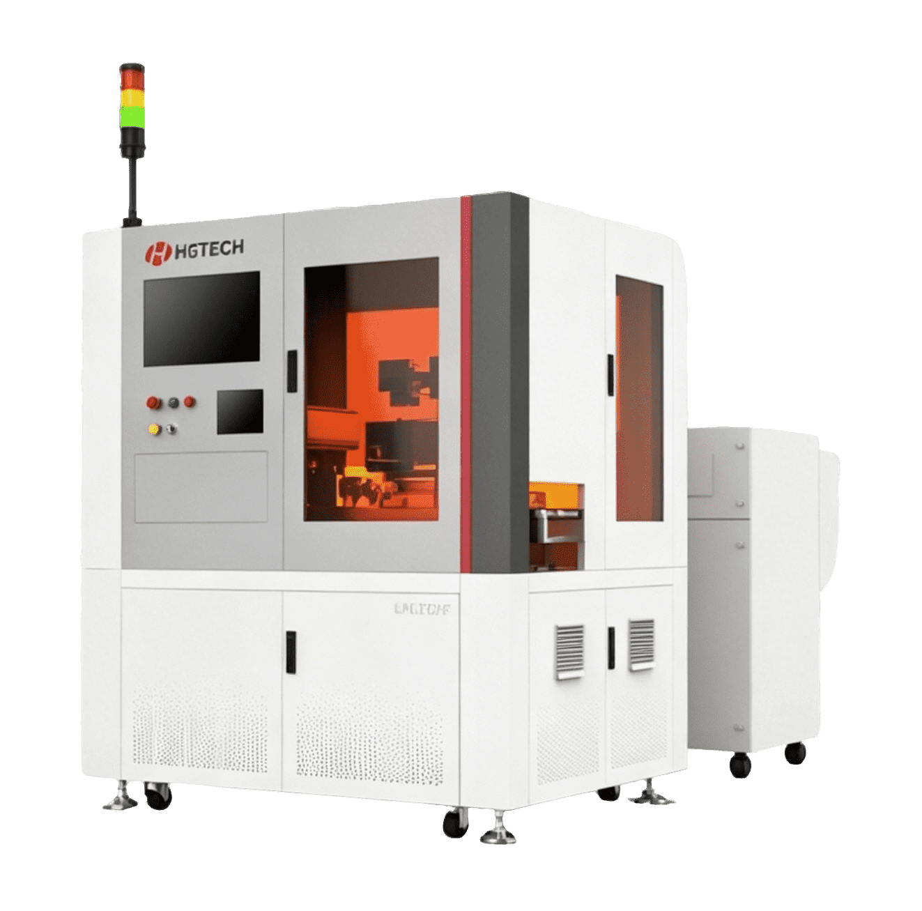
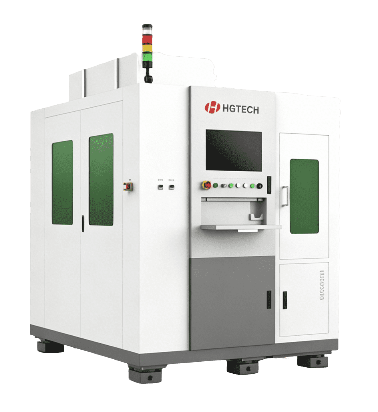
    Fully Automated Wafer Laser Annealing Machine
  • SiC Wafer Modification and Cutting

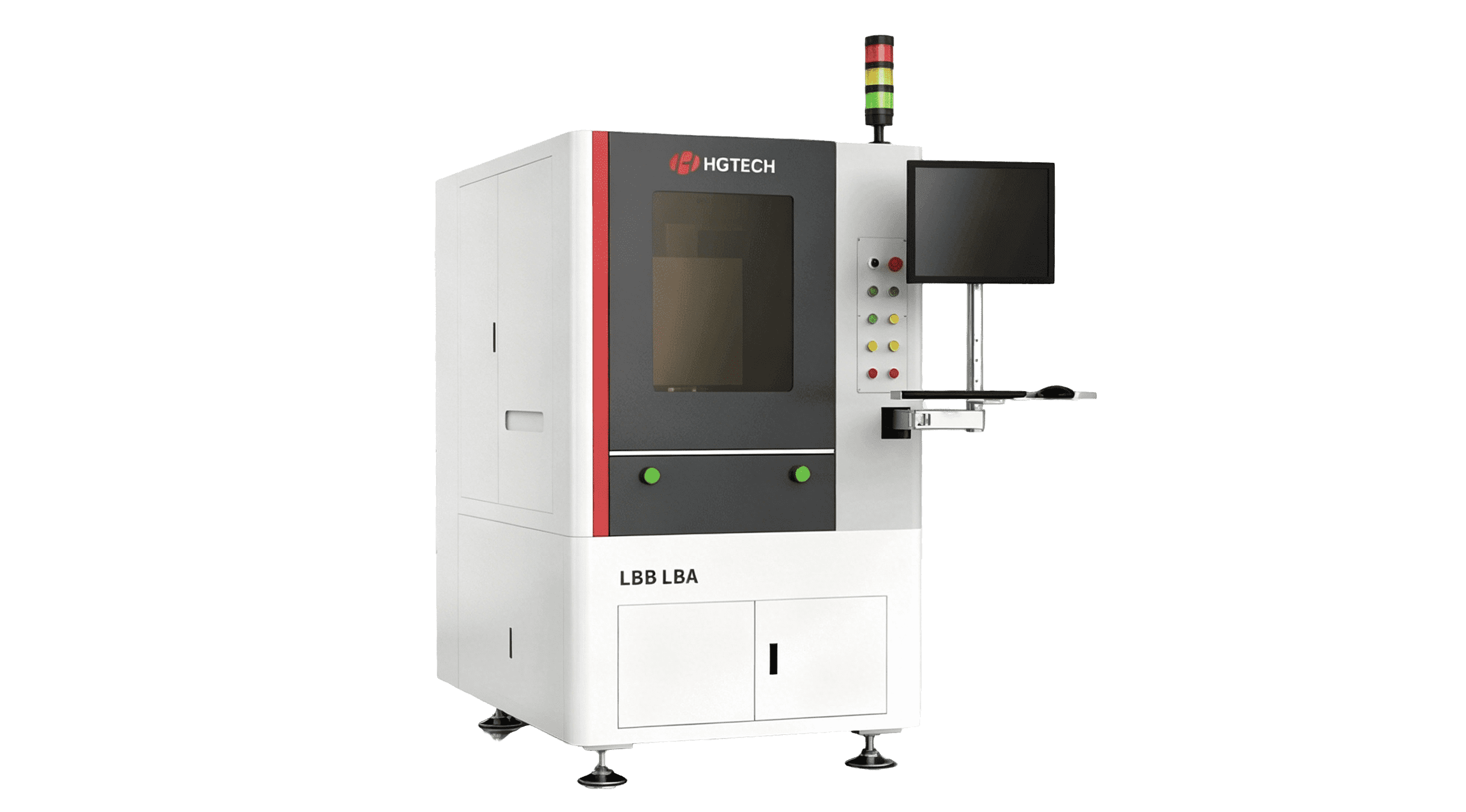
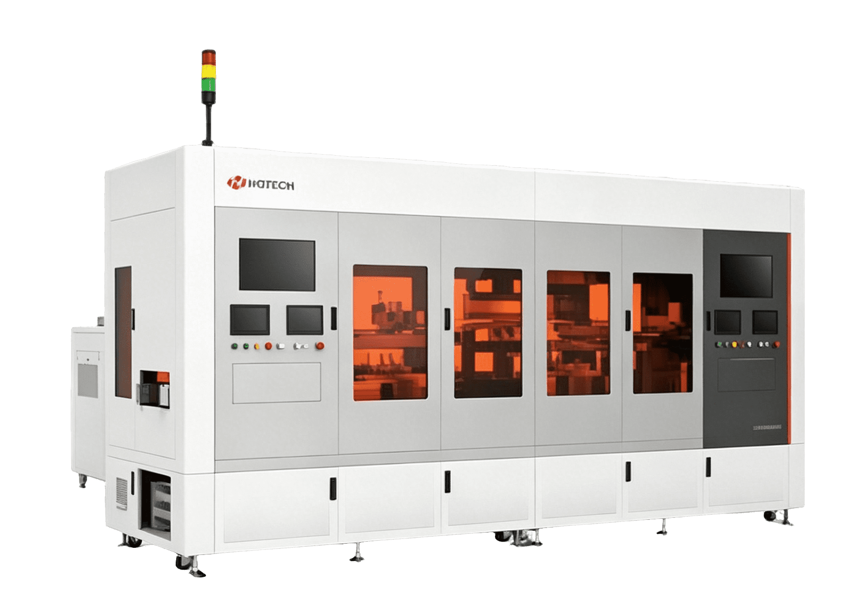
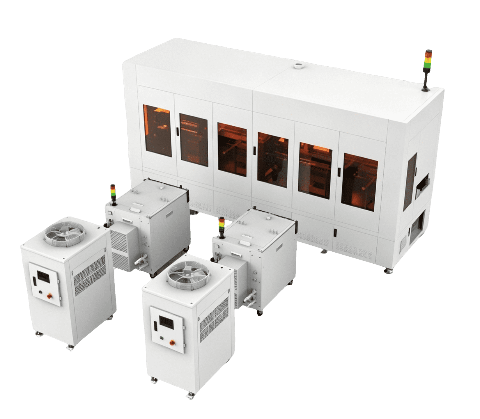
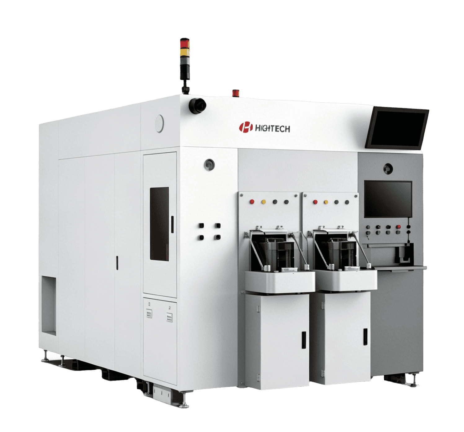
    SiC wafer modification and cutting solutions use custom ultrafast lasers, high-precision motion platforms, dynamic focus compensation, and vision positioning for stealth dicing and die separation.
    Value Points
    Suitable for 6–8 inch wafers | Supports internal modification and die separation | Uses vision positioning and automated wafer handling
    Recommended Products
    Fully Automatic SiC Wafer Modification and Cutting Equipment
  • Advanced SiC Processing

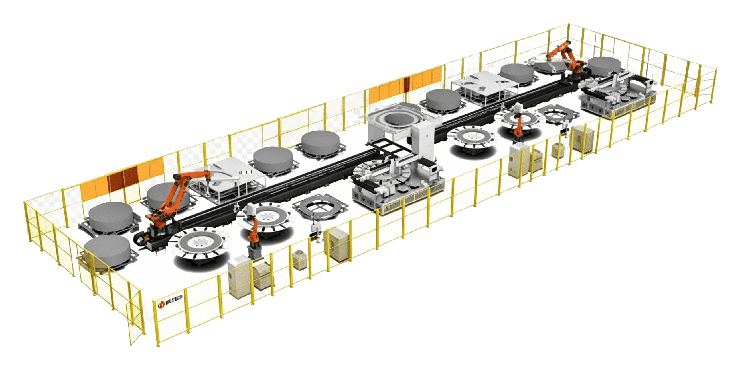
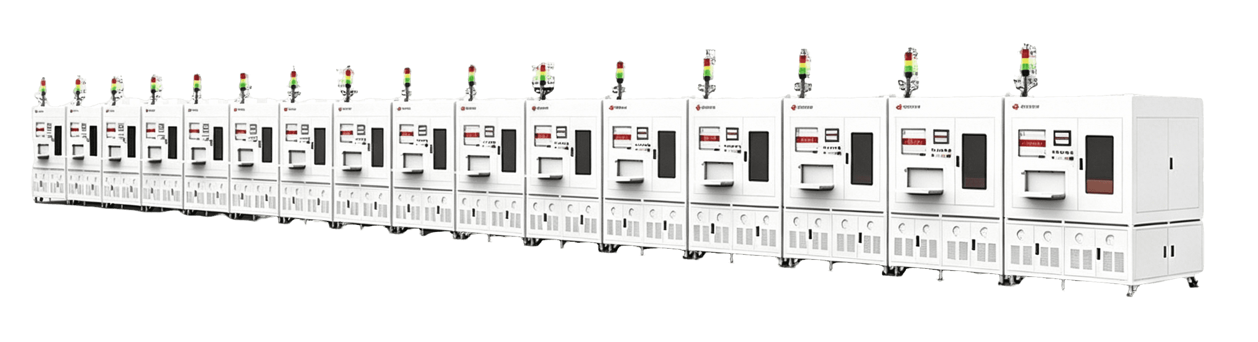
    SiC processing supports fully automatic wafer modification and cutting for 6–8 inch wafers, using ultrafast lasers, high-precision CCD vision, dynamic focus compensation, and automated wafer handling.
    Value Points
    Internal modification / stealth dicing | No front-side damage | Dynamic focus compensation | SEMI-standard automation | Supports advanced third-generation semiconductor manufacturing
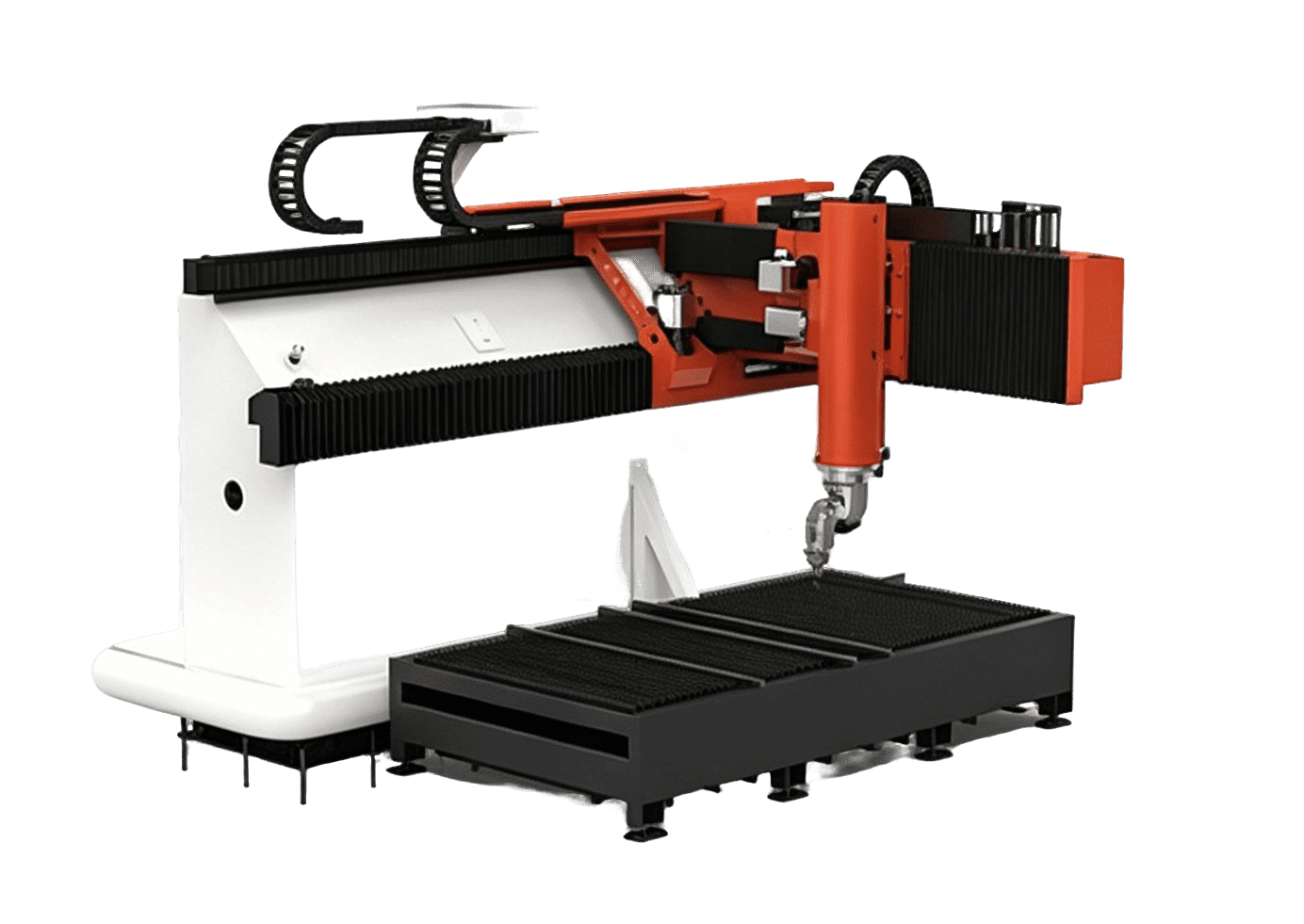
    Recommended Products
    Fully Automatic SiC Wafer Modification and Cutting Equipment
  • Wafer Laser Modified Cutting

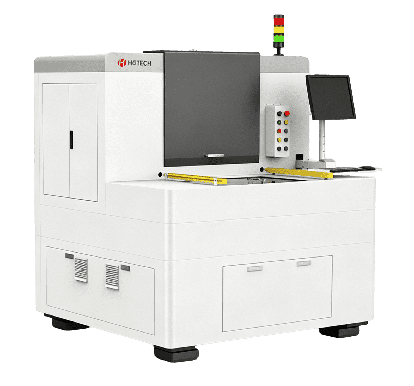
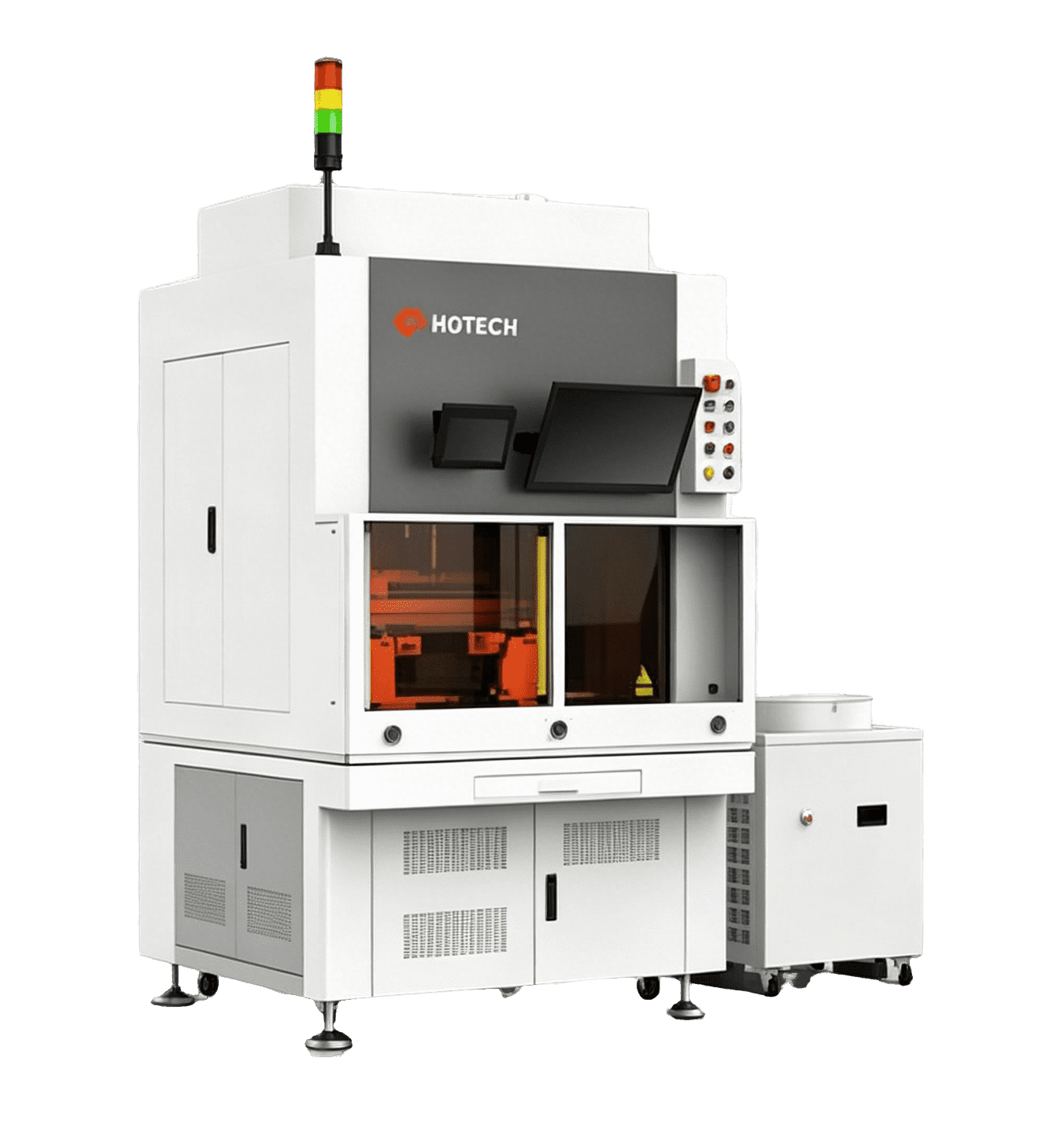
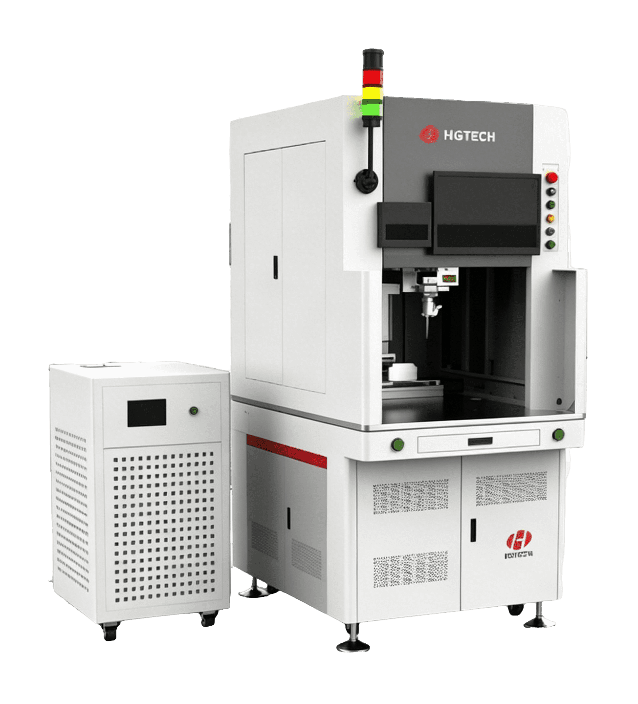
    Wafer laser modified cutting supports internal modified cutting of silicon-based wafers for 8-inch and above chip packaging and testing applications.
    Value Points
    High-quality modified cutting | Small edge collapse and low surface damage | Supports high-efficiency wafer separation
    Recommended Products
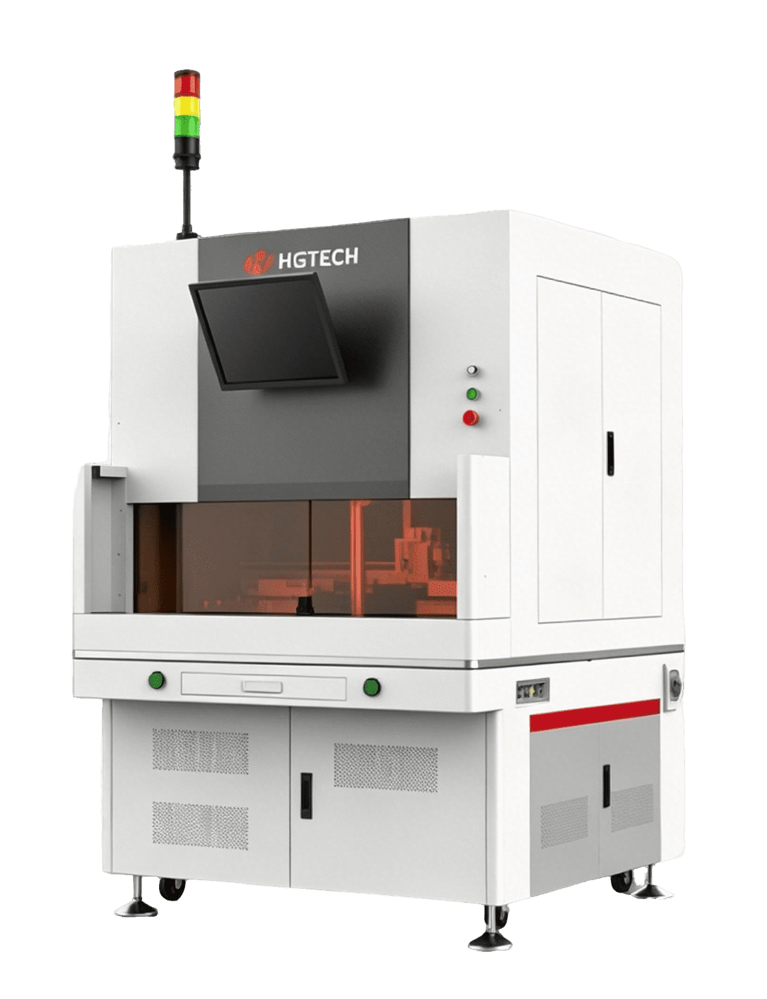
    Wafer Laser Modified Cutting Equipment
  • Wafer Slotting and Scribing

    Wafer slotting and laser scribing solutions support precision processing for low-k wafers, silicon-based GaN wafers, GPP wafers, and silicon or compound semiconductor wafers.
    Value Points
    Supports slotting and precision scribing | Suitable for semiconductor wafer processing | Covers nanosecond and picosecond scribing options
    Recommended Products
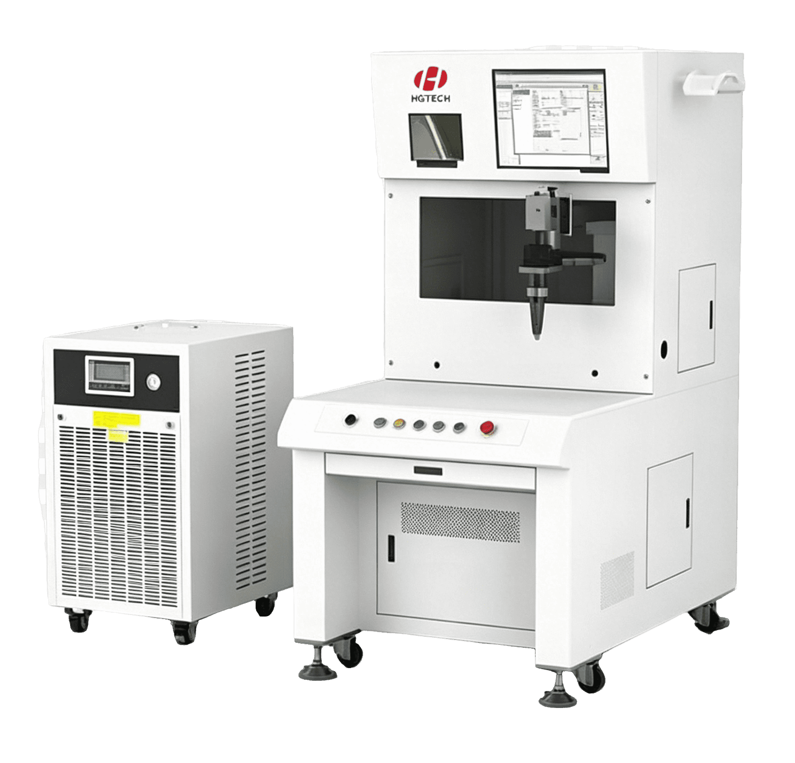
    Wafer Laser Slotting Equipment
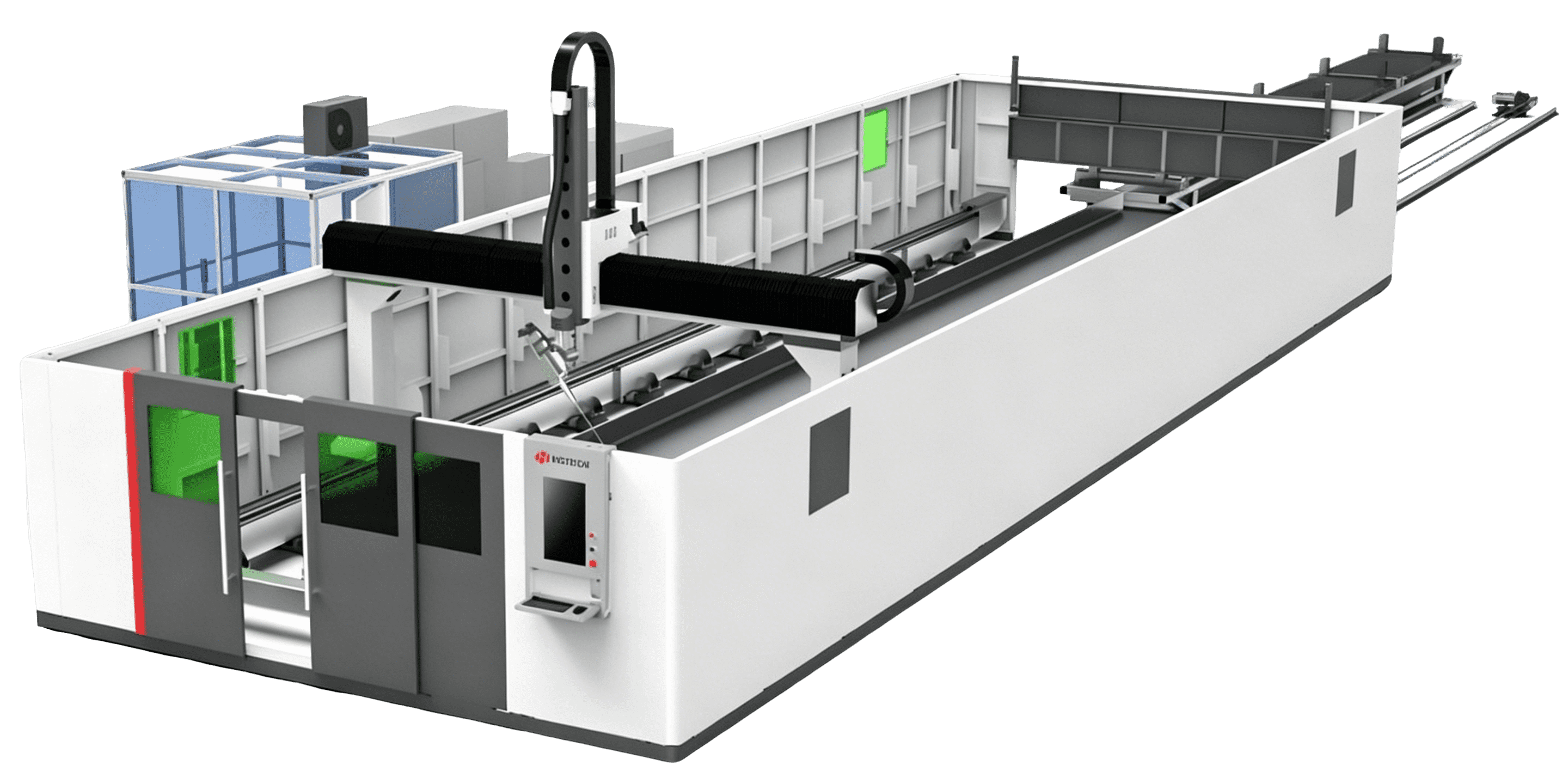
  • Automatic Wafer Laser Slotting Intelligent Equipment

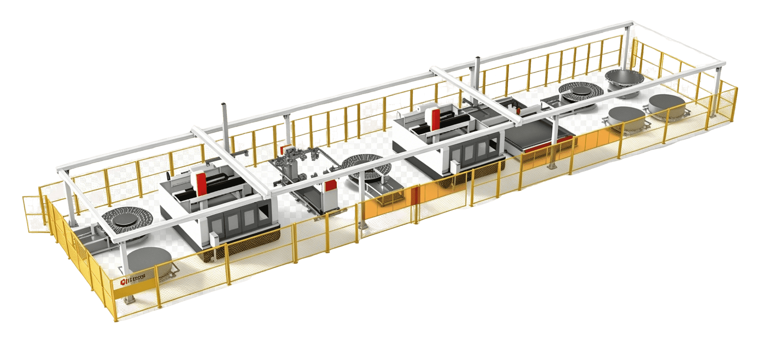
    Automatic wafer laser slotting equipment can support precision slotting and advanced wafer processing scenarios within semiconductor manufacturing.
    Value Points
    Wafer slotting | Precision laser processing | Semiconductor manufacturing support
    Recommended Products
    Wafer Laser Slotting Equipment
  • Wafer Marking and Traceability

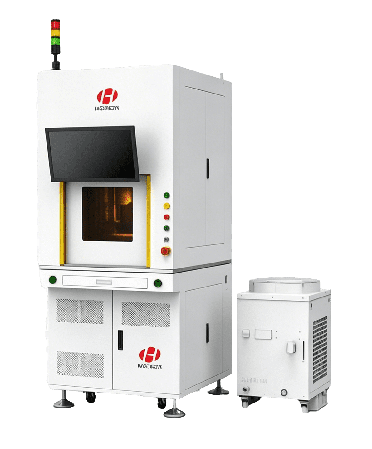
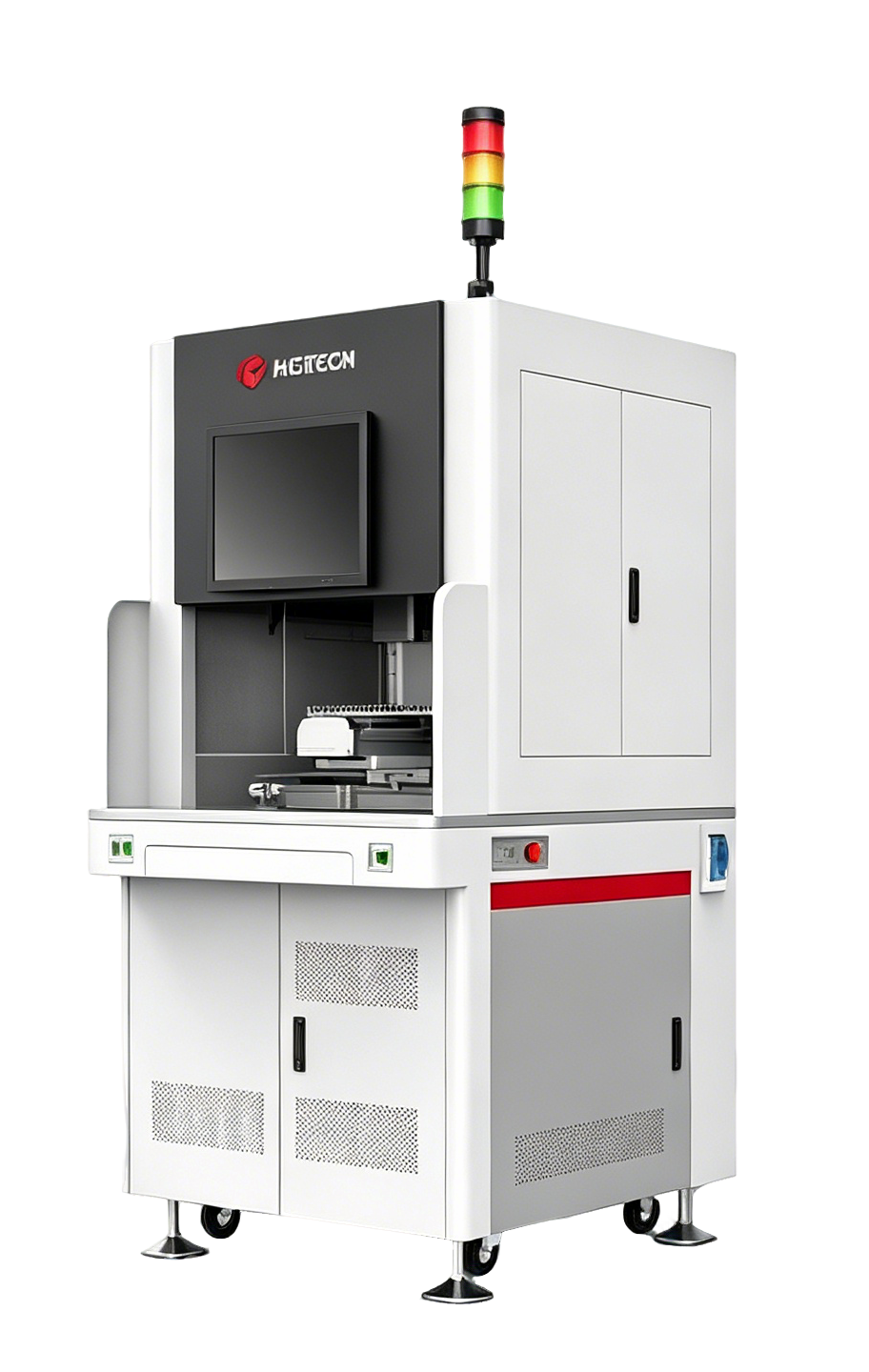
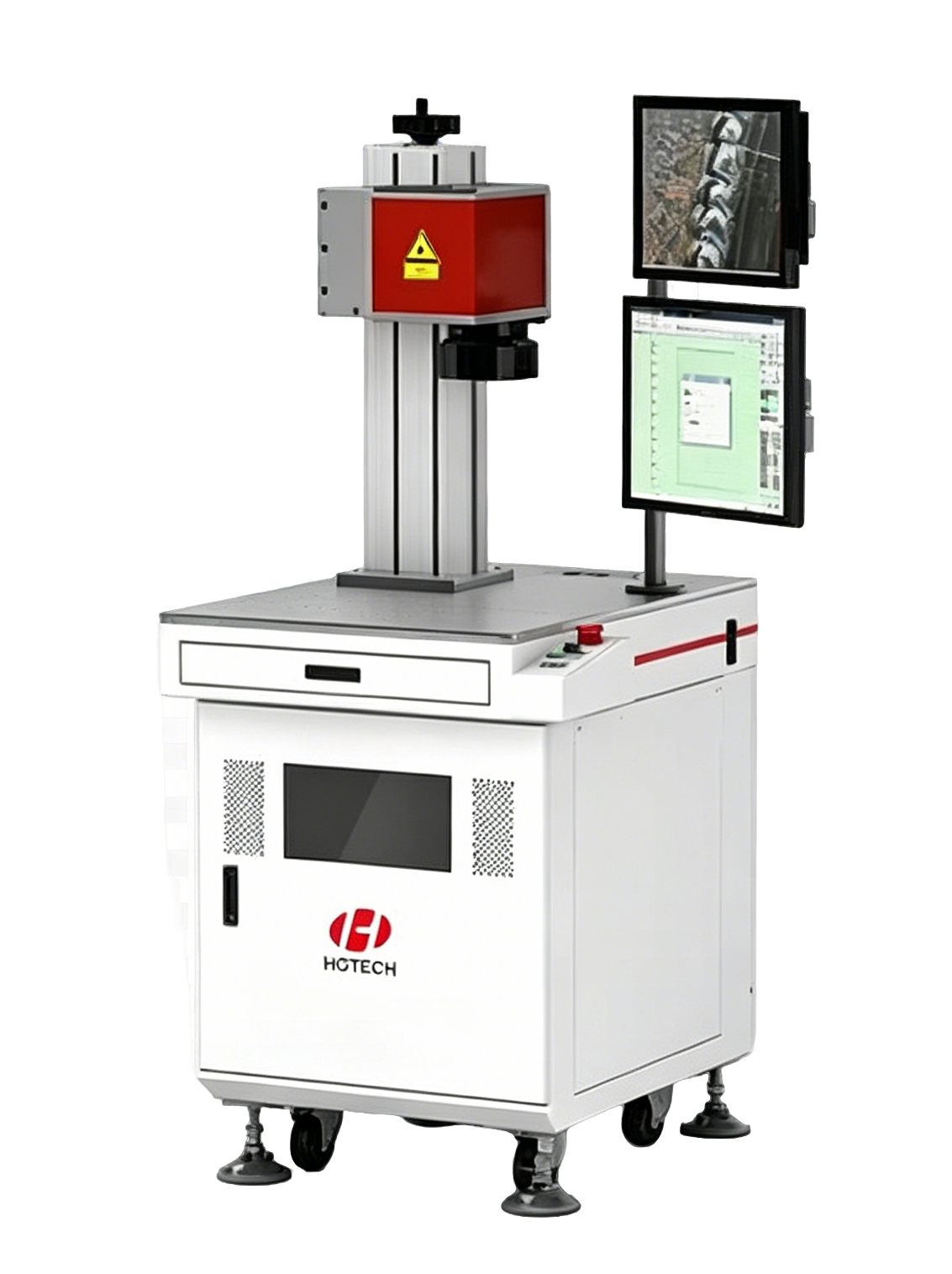
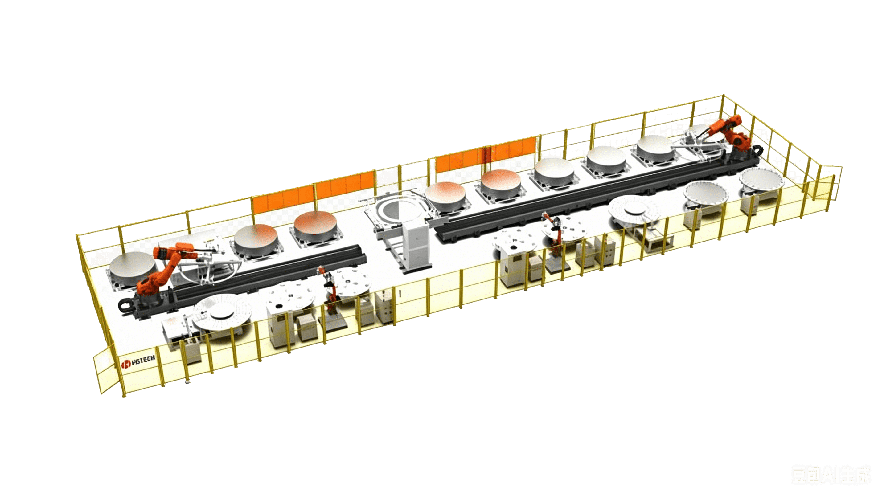
    Wafer laser marking solutions support full-automatic marking for semiconductor wafers using wafer handling, coaxial vision positioning, and laser marking technology.
    Value Points
    Supports 2–6 inch wafer marking | Automatic positioning and edge finding | Supports identification and traceability
    Recommended Products
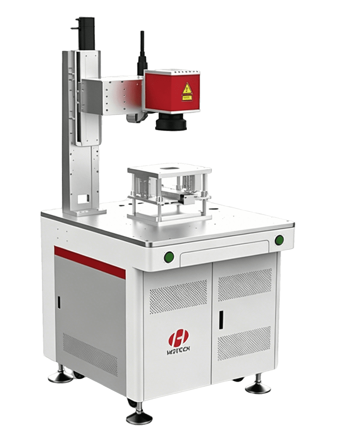
    Wafer Laser Marking Equipment
    Fully Automated Wafer Marking Equipment
  • Wafer Defect Detection

    Semiconductor wafer defect detection equipment supports inspection of patterned wafers and wafer surfaces for scratches, cracks, color differences, metal residue, and other defects.
    Value Points
    Suitable for 4–8 inch patterned wafers | Detects multiple surface defects | Supports high-resolution inspection
  • Substrate Defect Detection

    Semiconductor substrate defect detection equipment supports defect inspection for wafers, substrates, epitaxial wafers, and patterned wafers.
    Value Points
    Applicable to multiple wafer and substrate types | Detects particles, pits, scratches, stains, and cracks | Supports upstream and midstream quality control
  • Wafer Thickness Measurement

    Wafer thickness measuring equipment uses spectral confocal measurement to detect the size and flatness of semiconductor raw and epitaxial wafers.
    Value Points
    Supports raw and epitaxial wafer measurement | Focuses on size and flatness detection | Suitable for upstream semiconductor material production

Brittle Materials

Glass and Quartz Micro-Drilling

Glass and quartz micro-drilling solutions support high-yield processing of hard and brittle materials using picosecond or short-pulse laser technology.

Glass and Quartz Micro-Drilling

Glass and quartz micro-drilling solutions support high-yield processing of hard and brittle materials using picosecond or short-pulse laser technology.
Value Points
Suitable for glass and quartz | Supports micro-hole processing | Designed for stable continuous processing
System Modules

· Photovoltaic Glass Punching Equipment

Glass and Optical Material Cutting

Glass and optical material laser cutting solutions support precise, non-contact processing for brittle materials such as cover glass, optical glass, and related components.
Value Points
Non-contact cutting | Supports complex shapes | Suitable for glass and optical material processing
System Modules

· LightBlade Series

· Glass Laser Cutting Solutions

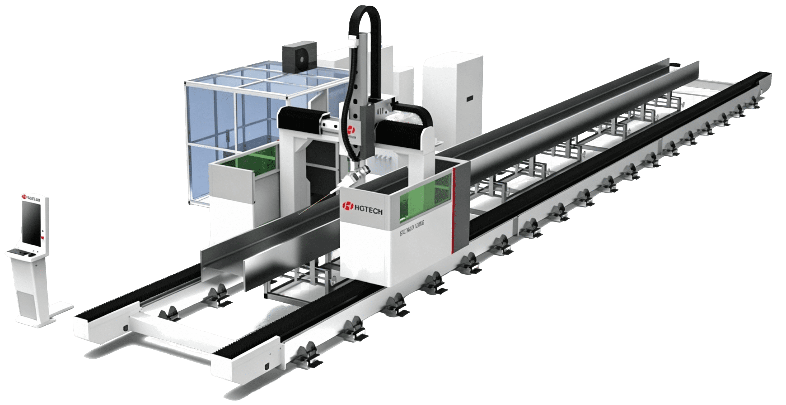
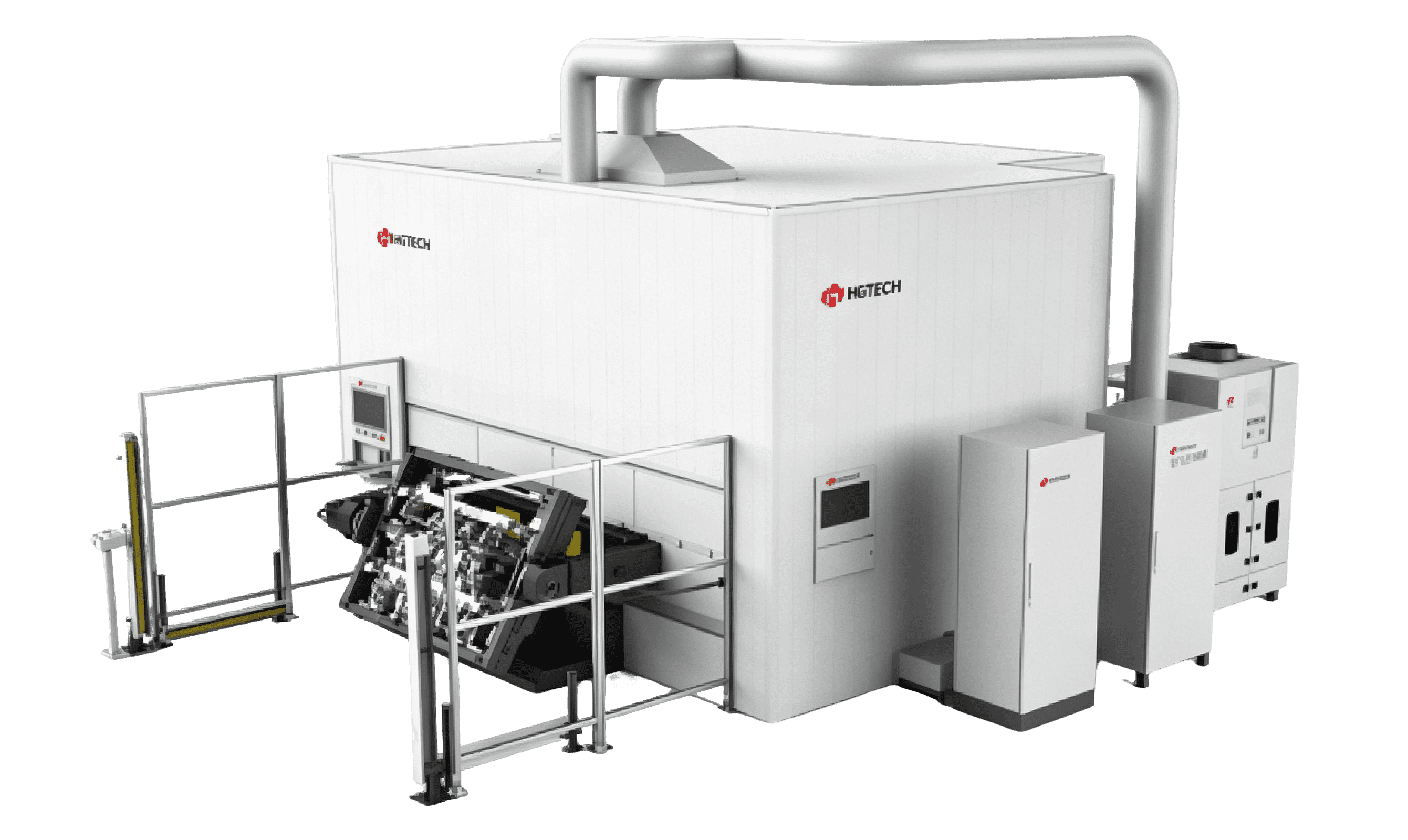
Glass Laser Welding for Transparent Materials

Ultrafast laser welding can support bonding of glass and transparent brittle materials without additional adhesives in selected precision manufacturing scenarios.
Value Points
Transparent material welding | No additional adhesive | Low thermal impact
System Modules

· Glass Laser Welding Solutions
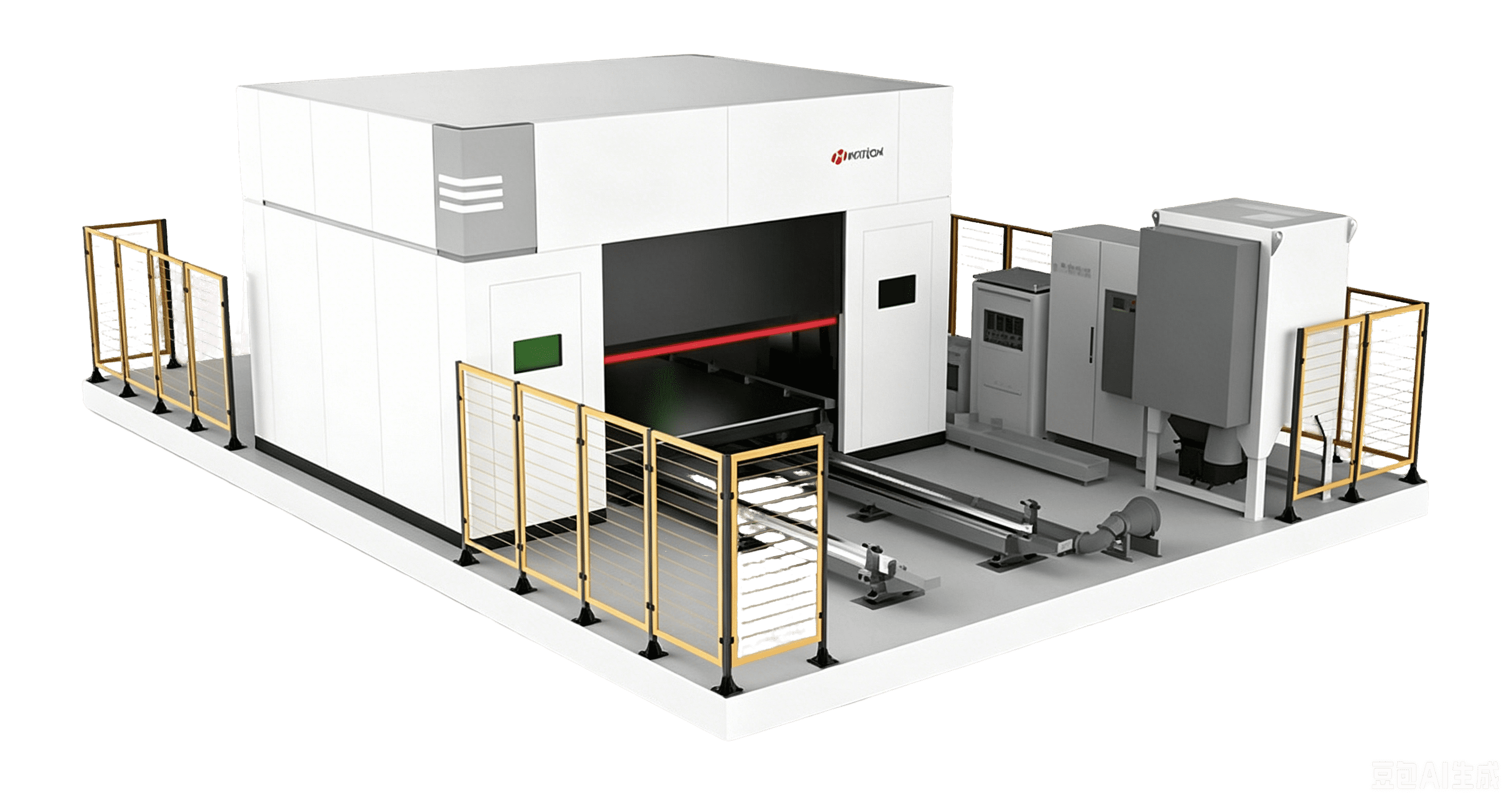
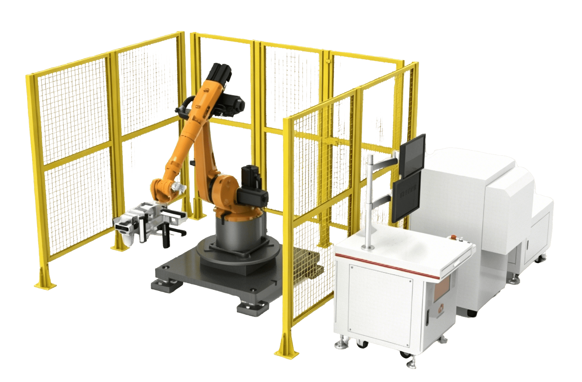
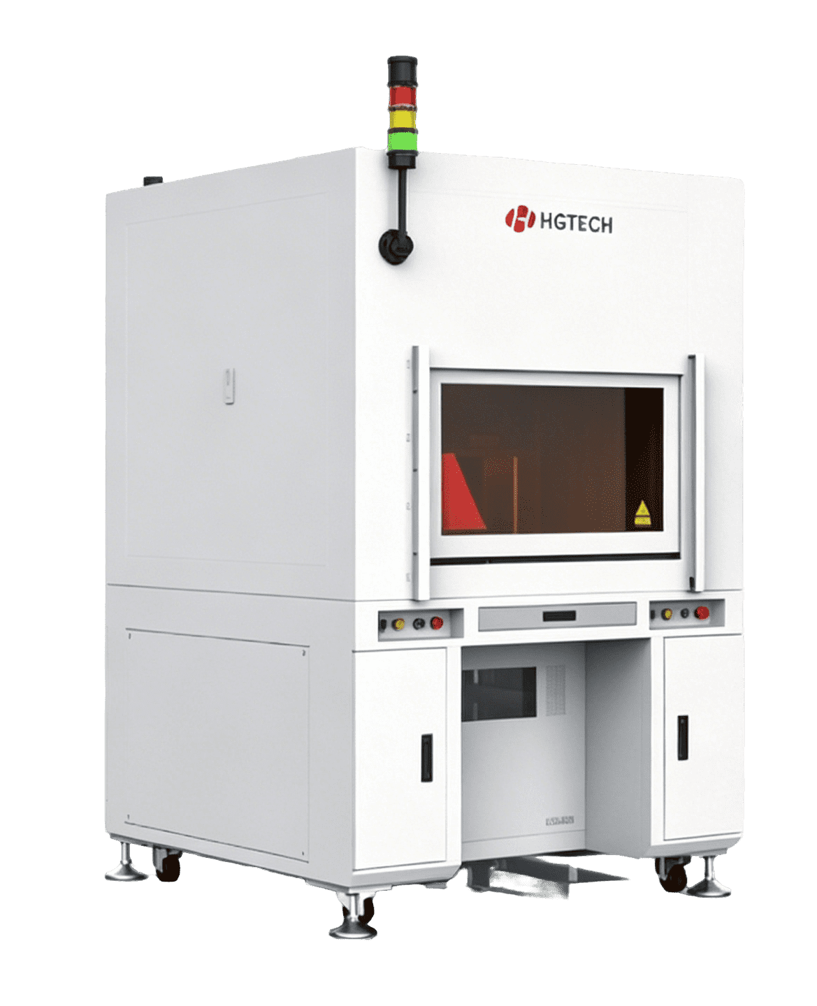
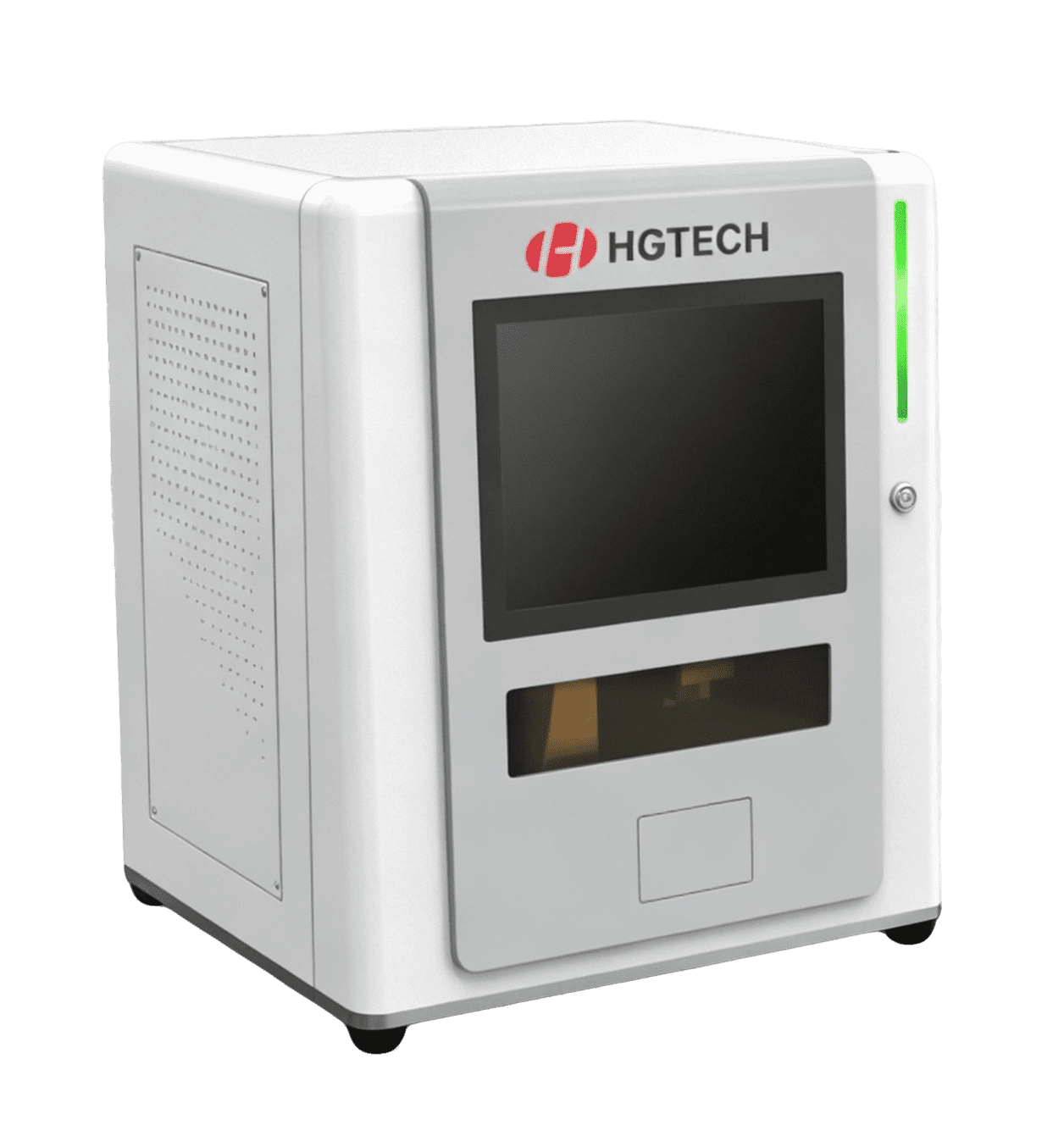
Ceramic Substrate Laser Cutting
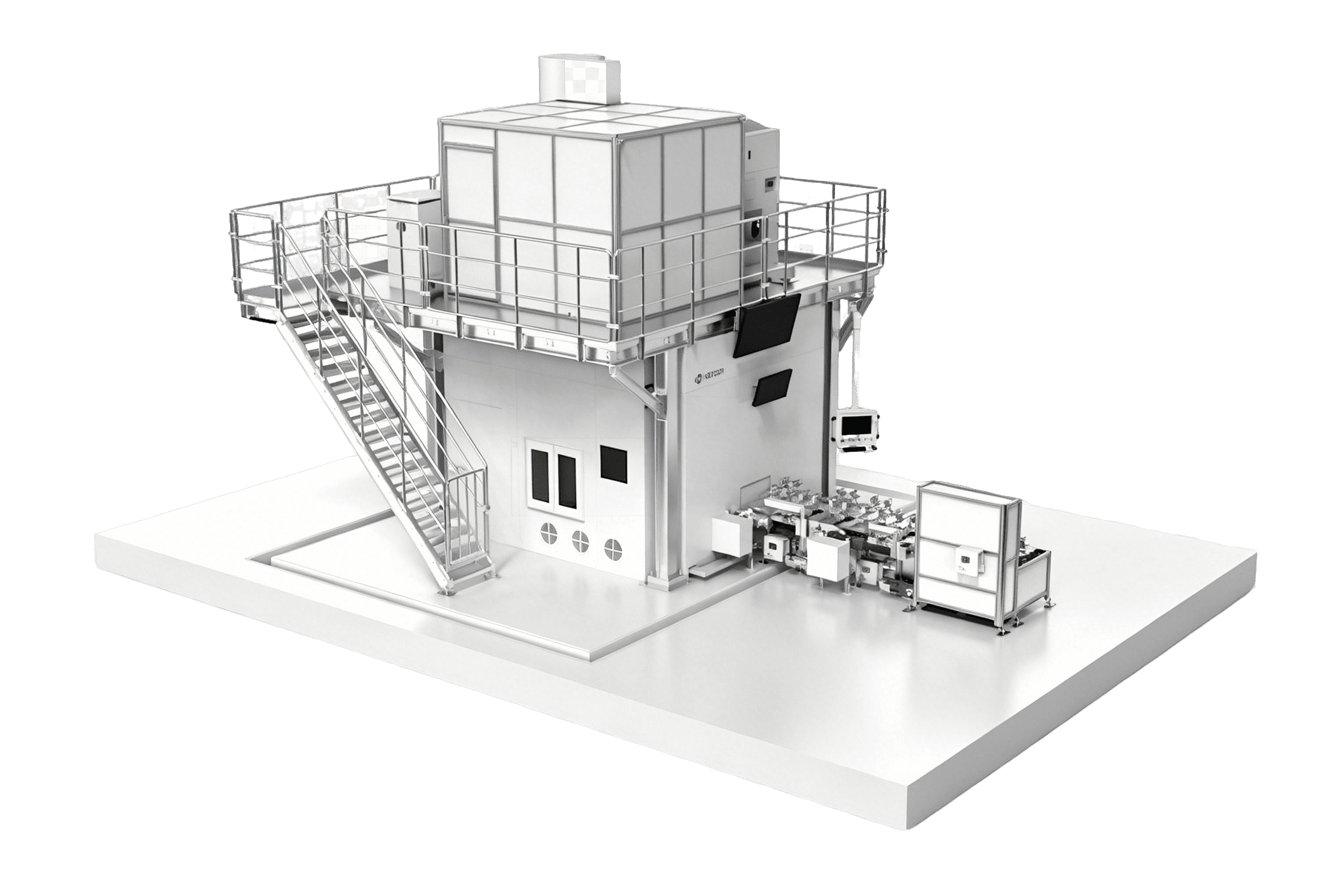
Ceramic substrate laser cutting solutions support high-efficiency and high-precision automatic processing for alumina, zirconium oxide, aluminum nitride, silicon nitride, and other ceramic materials.
Value Points
Suitable for ceramic substrates | Supports automatic loading and unloading | High-speed and high-precision processing
System Modules

· Ceramic Substrate Laser Cutting Series

Why HGTECH

Precision laser and inspection capabilities for semiconductor and brittle materials

GTECH combines wafer annealing, wafer cutting, marking, defect detection, thickness measurement, and brittle-material processing to support semiconductor and precision electronics manufacturing.
  • Wafer Processing

    Annealing, cutting, slotting, scribing, and marking
  • Inspection & Measurement

    Defect detection and thickness measurement
  • Brittle Material Processing

    Glass, quartz, optical glass, and ceramic substrate processing

Innovation Capability

  • 12
    National-Level Talent & Technology Platforms
  • 100+
    Scientific Research Achievement Awards
  • 3000+
    Independent Intellectual Property Rights

Innovative Achievements

  • In 2015, the project "Key Technologies and Complete Equipment for High-quality and High-efficiency Laser Welding and Cutting in Automobile Manufacturing" won the First Prize of the National Award for Progress in Science and Technology.
  • Since its establishment, it has obtained more than 100 national, provincial and ministerial scientific research achievement awards, including 4 National Awards for Progress in Science and Technology.
  • It has achieved over 70 "China’s Firsts" in the industry.
  • The average annual growth rate of authorized patents exceeded 28% in the past five years.
  • Led the formulation of the first international standard for China’s laser industry.
  • The average annual sales contribution rate of new products reached 41% over the past five years.
  • The National Enterprise Technology Center ranked 123rd among 1,744 evaluated institutions nationwide, topping the industry.

Discuss semiconductor wafer and brittle-material processing solutions

Connect with our team to explore wafer processing, inspection, measurement, and hard-brittle material laser solutions.