Wafer Defect Detection Series

Semiconductor Wafer Defect Detection Equipment

For the mid stream wafer manufacturing enterprises and downstream packaging and testing enterprises in the semiconductor industry chain, a multi-channel bright and dark field parallel detection system developed independently is adopted to detect the appearance defects of semiconductor wafers and grains with graphics.

Product Consultation

Name *
Company name *
E-mail *
Phone *
Country *
Main Business
  • Product Description

Product advantages:

  • Available in a variety of sizes

This equipment can be used for 4-8 inch patterned wafers

  • Can detect a variety of defects

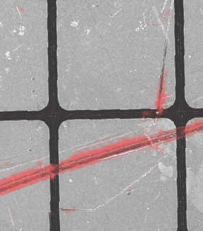
Detect defects such as scratch, back collapse, color difference, crack, scratch, metal residue and metal loss

  • High precision resolution

System resolution: 0.2-0.8 μ m

  • Fast detection speed

Patterned wafer: 15 minutes / wafer when the number of defects is less than 200

Sample display:

The gold plating layer falls off

defect detection machine

Crackle

defect detection machine

Coating surface detection

defect detection machine

Scratch

defect detection machine

  • Technical Parameters

Item Main parameters
General parameters Wafer size 4 ", 6" (Iron frame with blue film)
Number of boxes 2 pcs
Loading and unloading method Robot, mapping scanning
Motion platform X stroke 200mm, repetitive accuracy 10µm
Y stroke 45mm, repetitive accuracy 10µm
Z stroke 15mm, repetitive accuracy 5µm
Capacity 4", 25WPH 6", 20WPH
Test accuracy 3 µm
Detection performance Camera High resolution industrial camera
Lens Microlens
Light source Patented light source
Defect marking Automatic dotting
Power supply specification AC220V, 50Hz
Environment requirement Air source requirements 0.5-0.7Mpa compressed air, without obvious water vapor and grease
Using environment Temperature: 15-40 ℃. Humidity requirement: 30% - 70%, no frost
Overall size 2000mm*1200mm*2250mm

Message Form

Name *
Company name *
Country *
Main Business
E-mail *
Phone *
Specific Requirements *