
Automotive Industry
Laser Solutions for Automotive Manufacturing | HGLaser


 November 11, 2026
 10 Viewed
Driven by the rise of AI optical interconnects, silicon photonics chips are moving toward larger-format advanced processes, higher integration, and high-density bare-die arrays. Wafer value is high, dies are extremely small, and functional areas are densely packed. Die-level identification is no longer simply a matter of applying codes. It is a critical process requiring high precision, high cleanliness, and high stability. It connects the entire value chain from wafer fabrication to optical chips and optical modules, providing a reliable foundation for production quality control, end-to-end traceability, and data collaboration across the supply chain.
To address common challenges across the industry, HGLaser has developed a comprehensive laser processing solution for optoelectronic chips to systematically overcome the challenges of silicon photonics Die marking.
A silicon photonics SOI wafer has a three-layer vertical structure consisting of a top silicon layer, a BOX (buried oxide) layer, and a silicon substrate. Its surface is covered by a dense passivation layer that protects the performance of the optical waveguides.
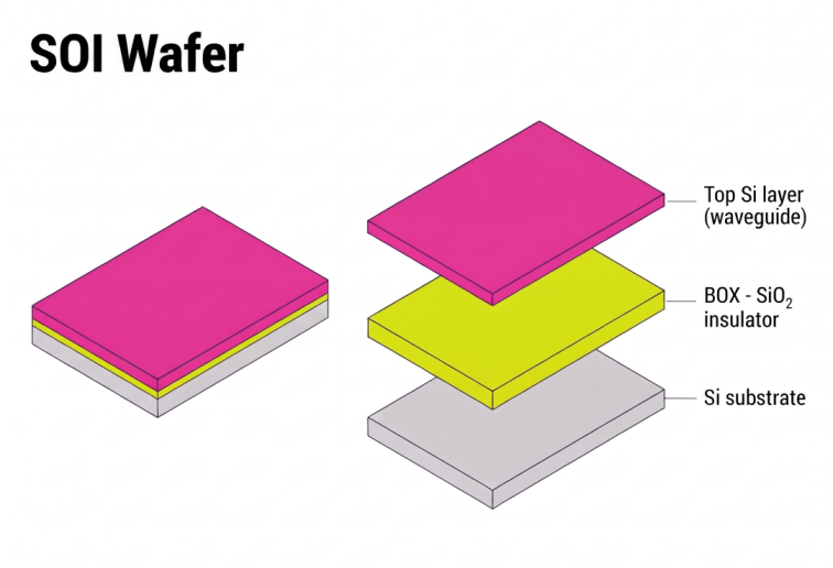
Hundreds or even tens of thousands of functional Dies are densely arranged in an array, with each Die corresponding to an independent photonic transmission unit. Markings must be confined to the limited space outside functional areas. They must not damage the waveguide structures, while remaining identifiable throughout the product lifecycle. Process difficulty increases exponentially as Die density rises.
High-density Die array marking must address three challenges simultaneously: consistent positioning across the entire array, data throughput for tens of thousands of Dies, and damage-free processing in densely packed layouts. Mass production requires a closed-loop capability covering wafer mapping, Die-by-Die positioning, path planning, and quality reinspection.
Silicon photonics wafer marking faces three major process challenges in mass production. Optimizing any single parameter alone is insufficient to support a stable production takt time on an unmanned 12-inch wafer production line.
With conventional single-mode positioning, deviations caused by wafer rotation and deformation accumulate across the array. Marking offsets on edge Dies can easily exceed tolerance limits. Even a micron-level deviation may intrude into an optical waveguide's functional area, resulting in chip scrap.
Limited Efficiency in Array-Based Processing
Each Die has a unique code. Conventional equipment imports data and positions and marks each Die individually. Its data throughput and path-planning efficiency cannot keep pace with array-based processing requirements or meet the production takt time of an unmanned 12-inch wafer line.
Conventional nanosecond lasers have a relatively large heat-affected zone. Because Dies are closely spaced, thermal stress can spread to neighboring Dies, causing sunburst-like stress patterns and lattice microcracks. Thermal damage to a single Die may trigger a chain effect in surrounding areas, and wafer-level yield loss can increase as Die density rises.
To address the marking challenges posed by high-density Die arrays on silicon photonics wafers, HGLaser Semiconductor draws on more than 30 years of laser technology expertise. It has developed an integrated, customized solution across three key areas: laser source, positioning, and data processing.
The solution systematically addresses the three core requirements of precision, efficiency, and yield.
A custom-developed laser source is used, with a pulse width far shorter than the material's thermal diffusion time. The heat-affected zone is controlled to within the micron scale, enabling damage-free 'cold' processing of the passivation layer. This prevents sunburst-like patterns, microcracks, and deformation of the buried oxide layer at the source, improving overall wafer yield.
A dual-vision positioning system combines global wafer mapping with microscopic positioning of individual Dies. Global vision calibrates the coordinates of every Die across the wafer array, while localized microscopic vision performs secondary alignment to compensate for deviations. This keeps Die marking positioning accuracy consistently within ±10 μm across the entire wafer, with a minimum character height as small as 30 μm, ensuring consistent marking throughout the array.
Equipped with a high-speed data processing engine, the system supports batch preloading of Die codes for the entire wafer array and automatically plans optimal marking paths to reduce repeated movements and idle travel. It supports batch generation of multiple code formats, including serial numbers, QR codes, and binary codes. Individual Die configuration is not required, significantly improving continuous processing efficiency and meeting the production takt time of unmanned 12-inch silicon photonics wafer lines.
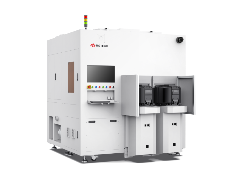
Designed for mass production of silicon photonics chips and memory chips, the system delivers high-precision, fully automated Die-level wafer laser marking with integrated marking and inspection, enabling traceability throughout the product lifecycle.
Ultra-High-Precision Marking: Positioning and marking accuracy of ±10 μm, with a minimum character height of 30 μm. Markings are consistent across the entire array and remain clear and readable.
Ultra-Clean, Damage-Free Marking: Particle-free and dust-free marking prevents wafer contamination and meets the cleanliness requirements of advanced silicon photonics processes.
Fully Automated Mass-Production Workflow: EFEM fully automated Loadport FOSB loading; supports overhead hoists/AGVs and SECS/GEM. Die codes can be preloaded in batches, with optimal path planning. OCR reinspects each Die and identifies defective locations, integrating marking and inspection in one process.
Comprehensive Compatibility: Supports marking on both the front and back of wafers and accommodates serial numbers, QR codes, binary dot-matrix codes, and other formats. Dot and character marking modes can be switched freely.
HGLaser's fully automated wafer laser Die marking system has been deployed at scale on 12-inch production lines at leading silicon photonics chip manufacturers. It consistently supports high-precision, high-yield, and high-efficiency marking of high-density Die arrays, serving as a key piece of equipment for the mass production of silicon photonics chips.
HGLaser Semiconductor will continue to focus on optoelectronic and semiconductor manufacturing. With precision marking capabilities covering materials across generations and wafers of all sizes, it aims to become a specialist in laser marking solutions for semiconductor materials across generations, providing high-precision laser processing solutions for silicon photonics and semiconductor manufacturing.
 share


